Method of forming DRAM access transistors

a technology of dram access transistor and dram, which is applied in the direction of transistors, electrical equipment, semiconductor devices, etc., can solve the problems of increasing the substrate doping density, reducing the threshold voltage, and/or the so-called short channel effect such as the punch-through phenomenon,

Inactive Publication Date: 2005-01-18
ROUND ROCK RES LLC
View PDF1 Cites 227 Cited by
  • Summary
  • Abstract
  • Description
  • Claims
  • Application Information

AI Technical Summary

Benefits of technology

Another embodiment of the present invention provides a self-aligned recessed gate structure for DRAM access transistors. The self-aligned recessed gate structure comprises a first recessed gate region located below a surface of a semiconductor substrate and having a width of about 35 nm to about 75 nm, more preferably of about 60 nm. The self-aligned recessed gate structure also comprises a second gate region extending above the surface of said semiconductor substrate by about 20 nm to about 800 nm. The second gate region has a width of about 50 nm to about 100 nm, more preferably of about 80 nm. Insulating spacers are located on sidewalls of the second gate region but not on sidewalls of the first recessed gate region.

Problems solved by technology

Recently, attempts to increase the packing density of cell capacitors and / or to simultaneously reduce the transistor size have been made but with limited results.
Unfortunately, reduction of the threshold voltage and / or the so-called short channel effect such as the punch-through phenomenon are likely to appear.
However, this approach increases the substrate doping density and requires reduction of the supply voltage, which in turn leads to reduction of the margin concerning the electric noise and fluctuations in the threshold voltage.
Higher channel doping causes degradation in retention time due to high electric field at the storage node junction.

Method used


Image

  • Method of forming DRAM access transistors
  • Method of forming DRAM access transistors
  • Method of forming DRAM access transistors

Examples


Embodiment Construction

In the following detailed description, reference is made to various specific exemplary embodiments in which the invention may be practiced. These embodiments are described with sufficient detail to enable those skilled in the art to practice the invention, and it is to be understood that other embodiments may be employed, and that structural, logical, and electrical changes may be made.

The terms “wafer” or “substrate” used in the following description may include any semiconductor-based structure that has a semiconductor surface. Wafer and structure must be understood to include silicon, silicon-on insulator (SOI), silicon-on sapphire (SOS), doped and undoped semiconductors, epitaxial layers of silicon supported by a base semiconductor foundation, and other semiconductor structures. The semiconductor need not be silicon-based. The semiconductor could be silicon-germanium, germanium, or gallium arsenide.

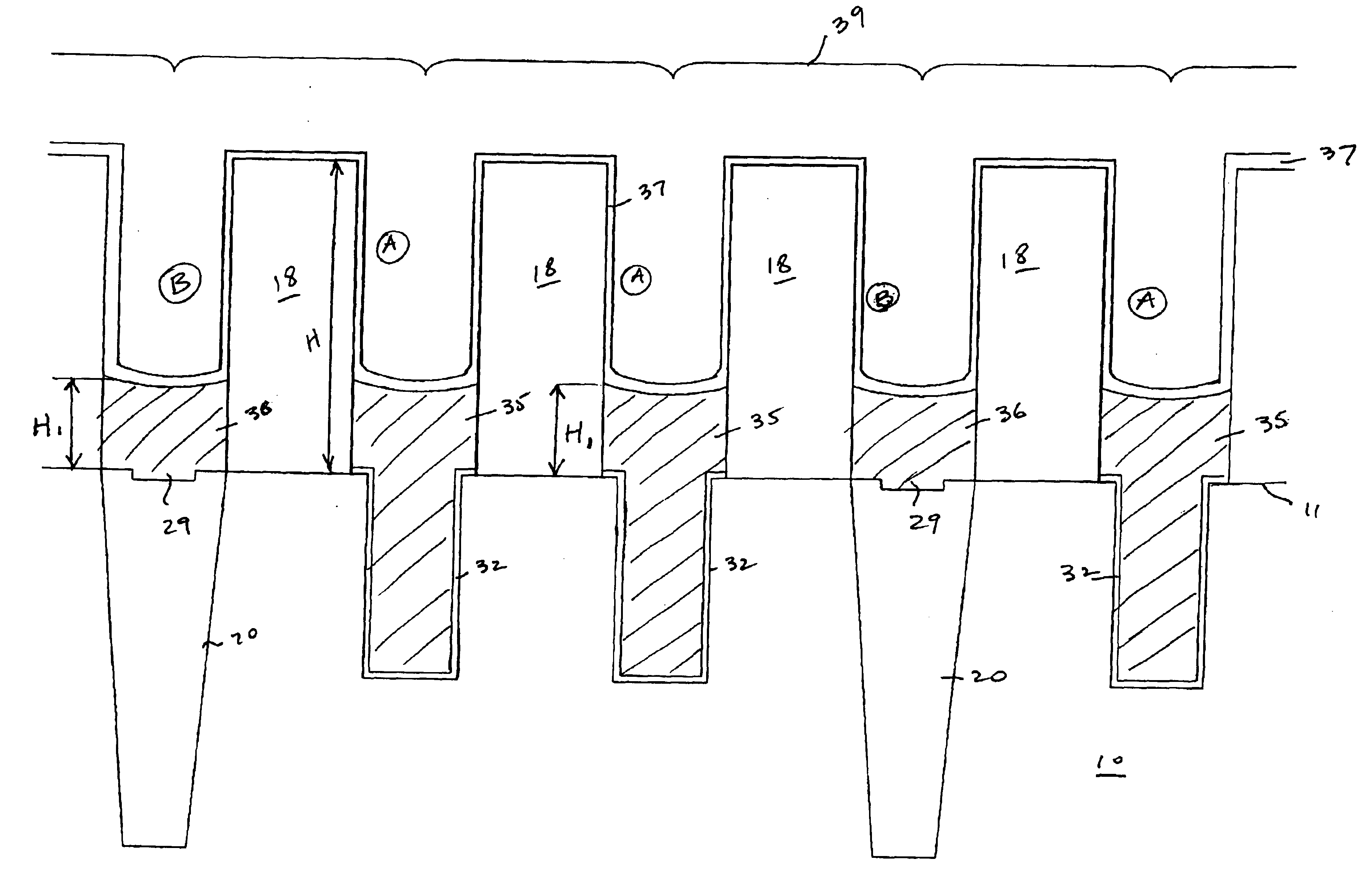
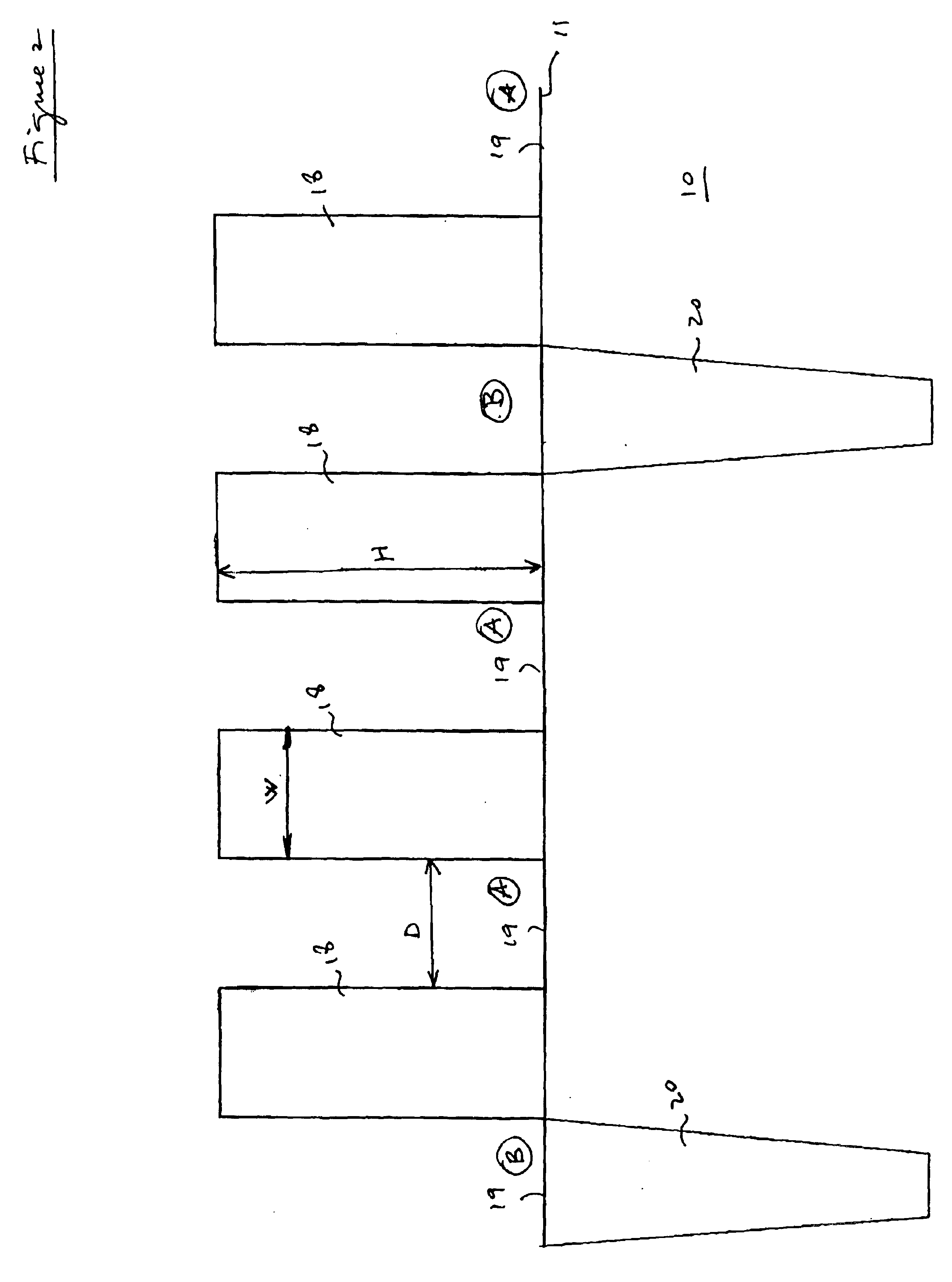
Referring now to the drawings, where like elements are designated by like referen...


PUM


Abstract

Self-aligned recessed gate structures and method of formation are disclosed. Field oxide areas for isolation are first formed in a semiconductor substrate. A plurality of columns are defined in an insulating layer formed over the semiconductor substrate subsequent to which a thin sacrificial oxide layer is formed over exposed regions of the semiconductor substrate but not over the field oxide areas. A dielectric material is then provided on sidewalls of each column and over portions of the sacrificial oxide layer and of the field oxide areas. A first etch is conducted to form a first set of trenches within the semiconductor substrate and a plurality of recesses within the field oxide areas. A second etch is conducted to remove dielectric residue remaining on the sidewalls of the columns and to form a second set of trenches. Polysilicon is then deposited within the second set of trenches and within the recesses to form recessed conductive gates.

Description

FIELD OF THE INVENTIONThe present invention relates to dynamic random access memory (DRAM) cells and, in particular, to a novel process for their formation.BACKGROUND OF THE INVENTIONA dynamic random access memory cell typically comprises a charge storage capacitor (or cell capacitor) coupled to an access device, such as a Metal-Oxide-Semiconductor Field Effect Transistor (MOSFET). The MOSFET functions to apply or remove charge on the capacitor, thus affecting a logical state defined by the stored charge. The amount of charge stored on the capacitor is determined by the electrode (or storage node) area and the interelectrode spacing. The conditions of DRAM operation such as operating voltage, leakage rate and refresh rate, will generally mandate that a certain minimum charge be stored by the capacitor.In the continuing trend to higher memory capacity, the packing of storage cells must increase, yet each must maintain required capacitance levels. This is a crucial demand of DRAM fabr...

Claims


Application Information

Patent Timeline
Patent Type & Authority Patents(United States)
IPC IPC(8): H01L21/02H01L21/70H01L21/336H01L21/8234H01L21/8242H01L27/108
CPCH01L27/10876H01L29/7835H01L29/66621H01L29/7834H01L27/10808H01L27/10811H01L29/42376H01L27/10891H10B12/312H10B12/31H10B12/053H10B12/488H10B99/00H10B12/00
Inventor TRAN, LUAN C.
Owner ROUND ROCK RES LLC
Why Eureka
Try Eureka