

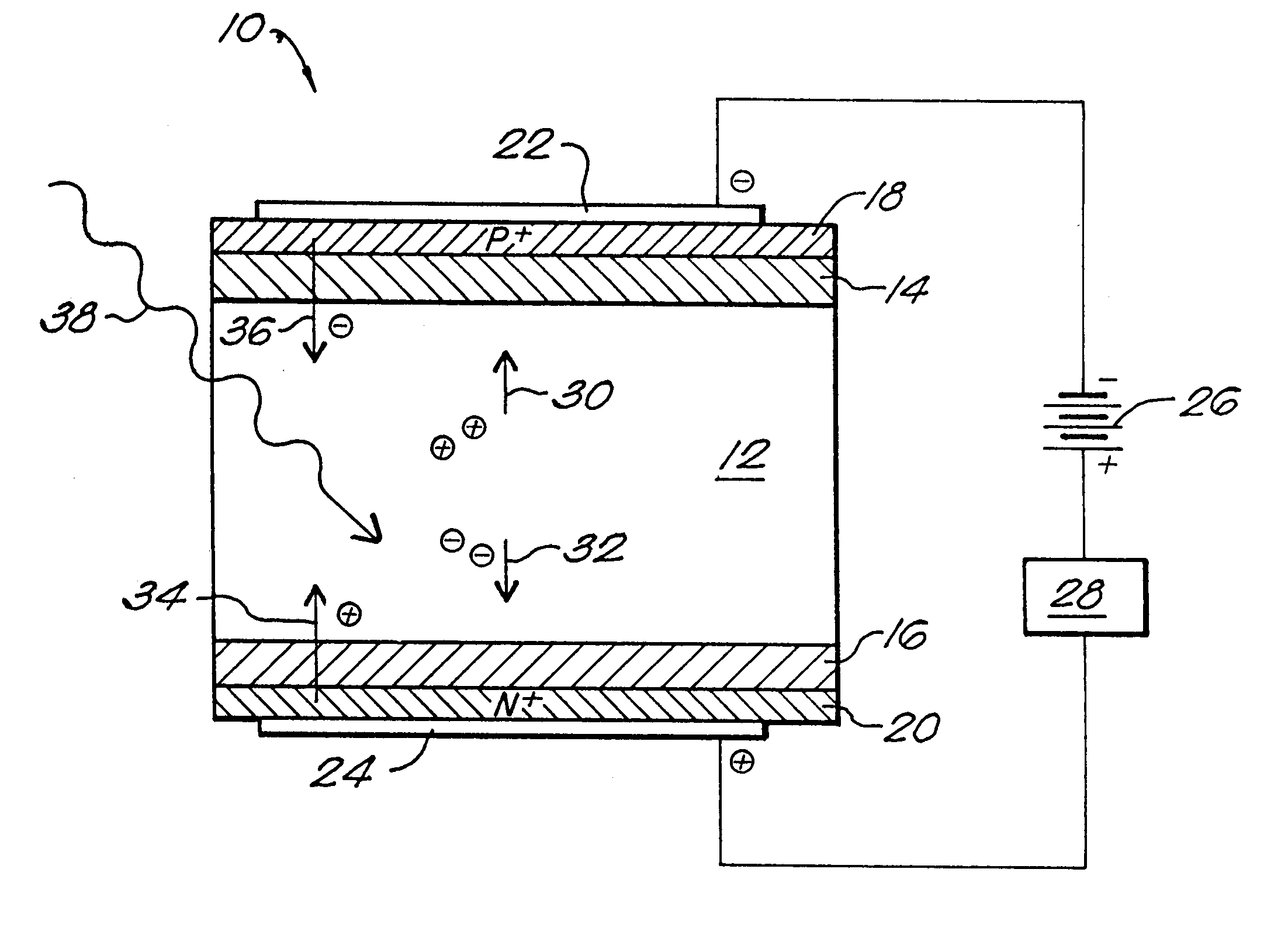
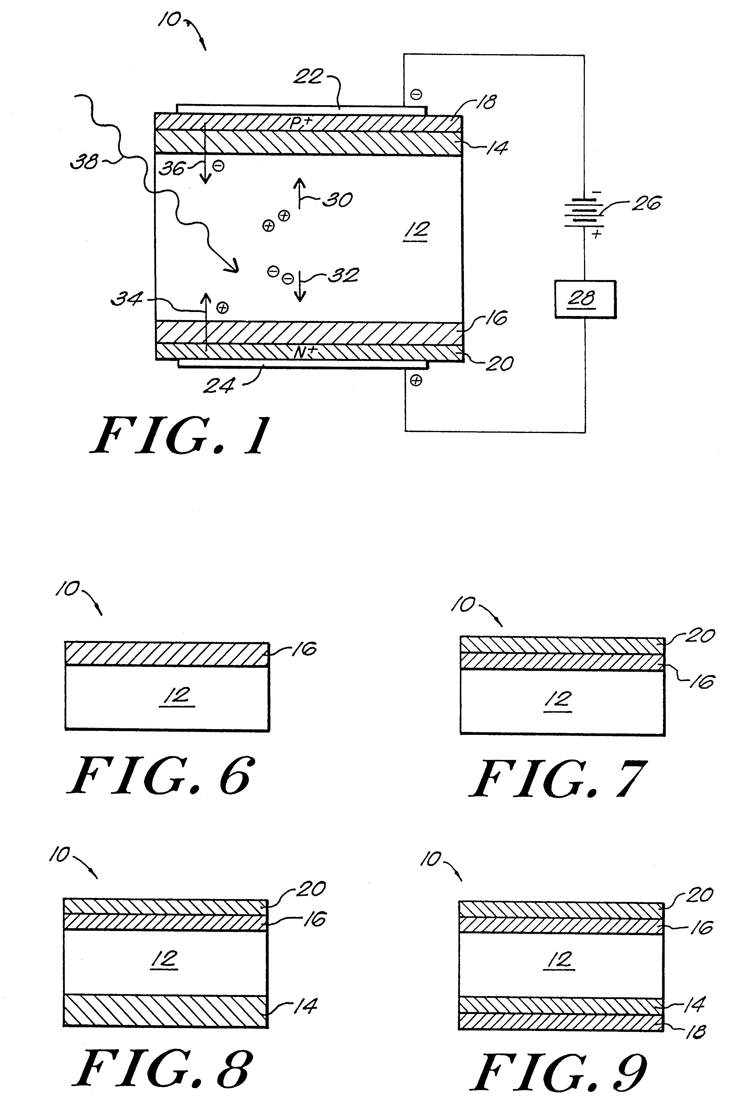
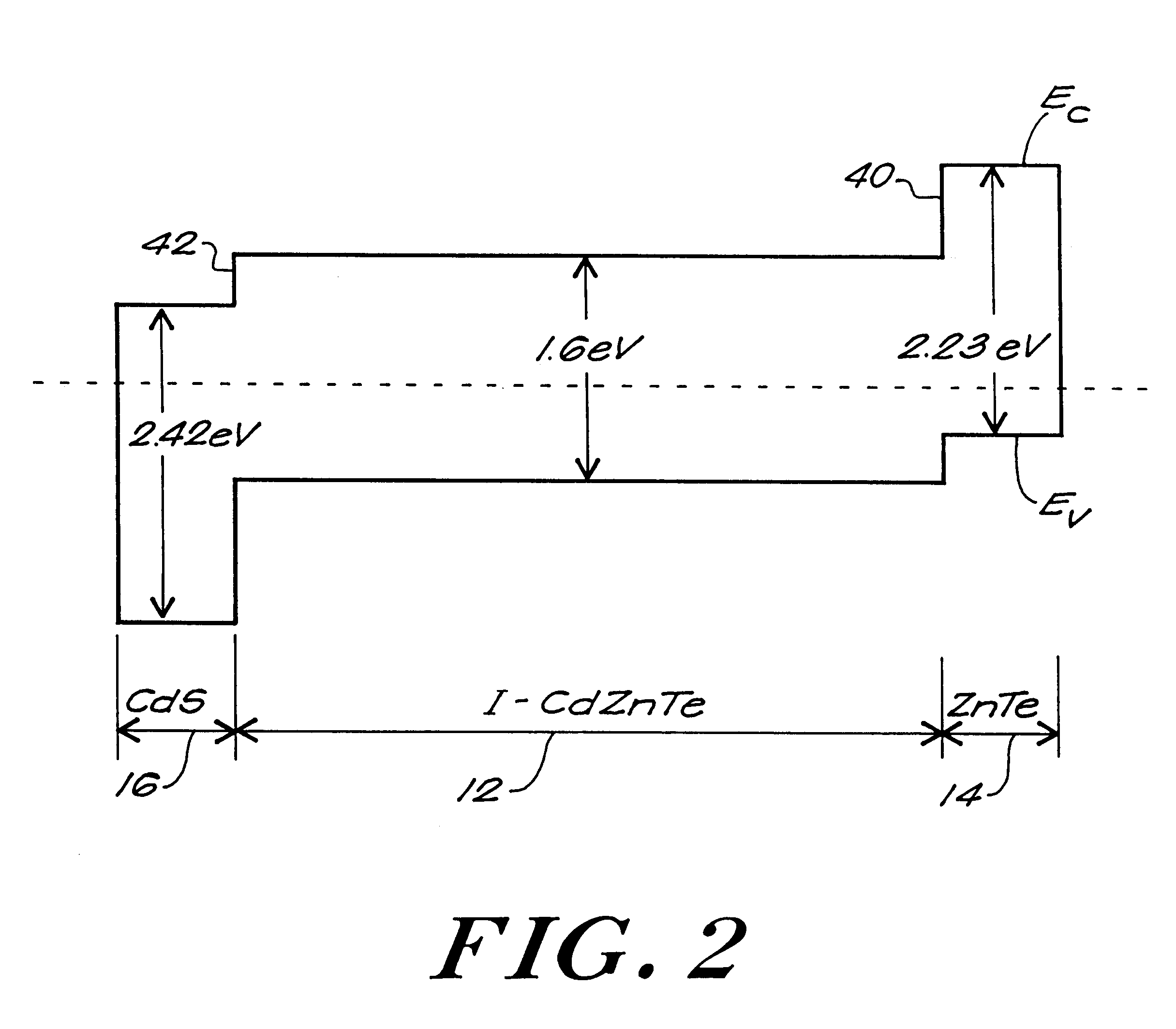
Semiconductor P-I-N detector
a technology of magnetoductor and detector, which is applied in the field of high-energy radiation detection, can solve the problems of msm detectors suffering from particular drawbacks, known high-energy detectors that are not suitable for use in gamma ray spectrometers operating at room temperature, and fail to provide acceptable energy resolution while operating at room temperature. , to achieve the effect of reducing the diffusion of dopant, reducing the leakage current, and reducing the diffusion of dop
- Summary
- Abstract
- Description
- Claims
- Application Information
AI Technical Summary
Benefits of technology
Problems solved by technology
Method used
Image

Examples
example
For P-I-N fabrication, CdZnTe crystals were grown using a High Pressure Bridgeman method. The crystals grown have a resistivity on the order of 10.sup.10 ohms-cm. Prior to the deposition of the CdS and ZnTe layers onto the CdZnTe layer, the CdZnTe crystals were etched in a bromine methanol solution and samples were immediately transferred to a vacuum evaporation system.
Next, an approximately 1 micron thick CdS layer was deposited on the CdZnTe at a substrate temperature of 125.degree. C. Thereafter, a 0.5 micron thick indium layer was evaporated as a contact layer to the CdS. On the other side of the CdZnTe crystal, an approximately 1 micron thick ZnTe layer was deposited. After the deposition of the ZnTe, the ZnTe layer was doped with copper that extended 0.25 micrometers into the underlying ZnTe boundary layer. Finally, a 0.5 micron thick gold layer was evaporated on the copper doped ZnTe layer as a contact layer. The ZnTe layer was evaporated at a substrate temperature of 100.deg...
PUM
 Abstract
Description
Claims
Application Information