Method to fabricate a strained Si CMOS structure using selective epitaxial deposition of Si after device isolation formation

a technology of strained si and cmos, which is applied in the direction of semiconductor devices, electrical equipment, transistors, etc., can solve the problems of reducing the performance enhancement, strained layer needs to be protected from high-temperature processing, and strained layer degrading device properties,

Inactive Publication Date: 2002-08-06
SAMSUNG ELECTRONICS CO LTD
View PDF16 Cites 271 Cited by
  • Summary
  • Abstract
  • Description
  • Claims
  • Application Information

AI Technical Summary

Benefits of technology

One object of the present invention is to provide a strained Si CMOS device wherein the strained Si layer is not adversely affected by high-thermal budget processing steps.
Another object of the present invention is to provide a strained Si CMOS device in which the strained Si layer is not consumed by processing steps that are known to consume Si in the active device areas, thereby minimizing the required thickness of the strained Si layer.

Problems solved by technology

One of the difficulties in realizing strained Si CMOS technology is that the strained layer needs to be protected from high-temperature processing steps during the fabrication process.
Moreover, ion implantation, which is typically used in well formation, may damage the strained Si layer degrading the device properties and diminishing the performance enhancements that can be advantageously obtained when using strained Si layers.
However, various processing steps including oxidation and etching (e.g., chemical etching and dry etching) consume the top Si layer; thus, in present processing of strained CMOS devices, the epitaxially strained Si layer has to be sufficiently thick to cover the potential thickness loss that may occur during oxidation and / or etching.

Method used


Image

  • Method to fabricate a strained Si CMOS structure using selective epitaxial deposition of Si after device isolation formation
  • Method to fabricate a strained Si CMOS structure using selective epitaxial deposition of Si after device isolation formation
  • Method to fabricate a strained Si CMOS structure using selective epitaxial deposition of Si after device isolation formation

Examples


Embodiment Construction

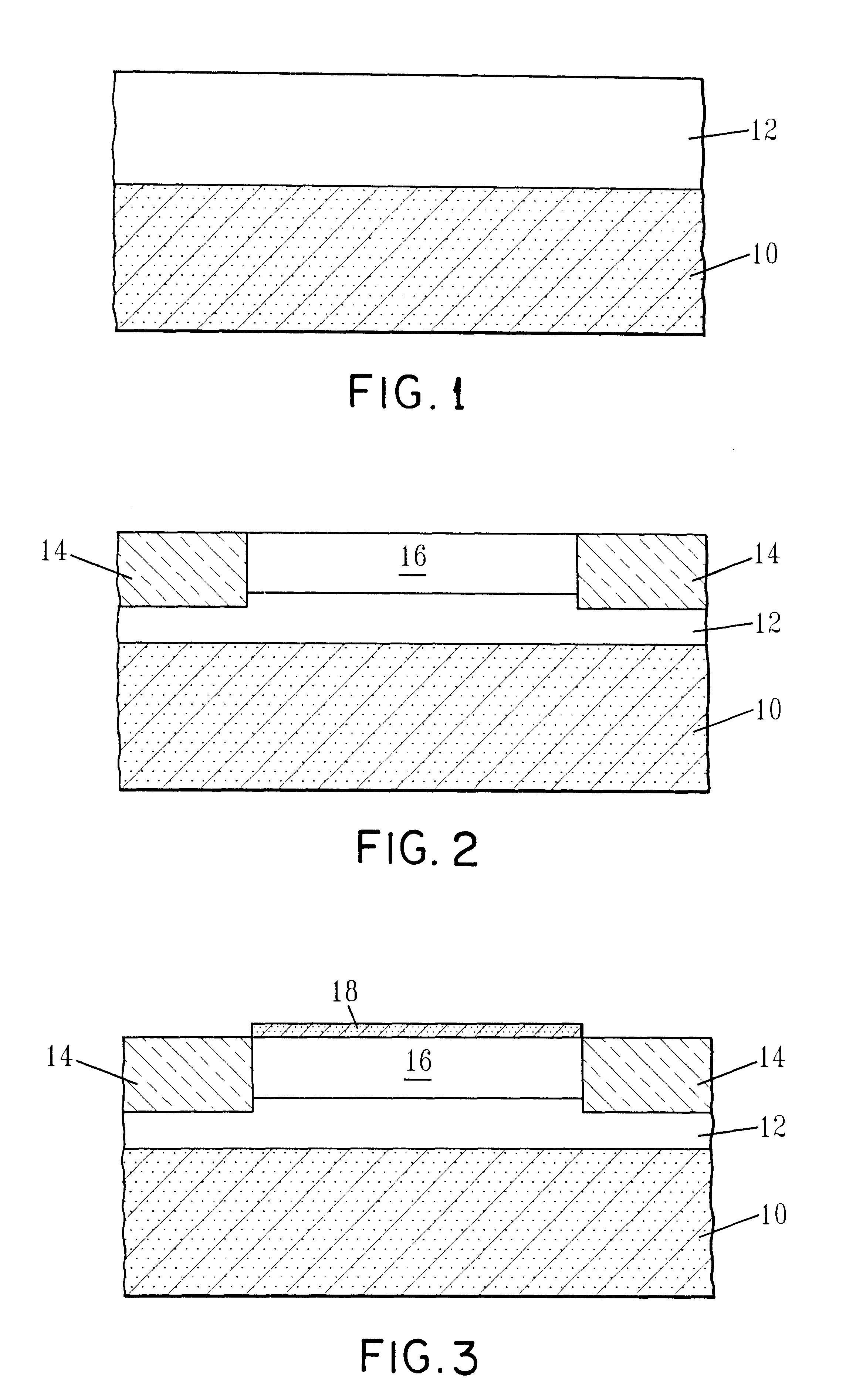
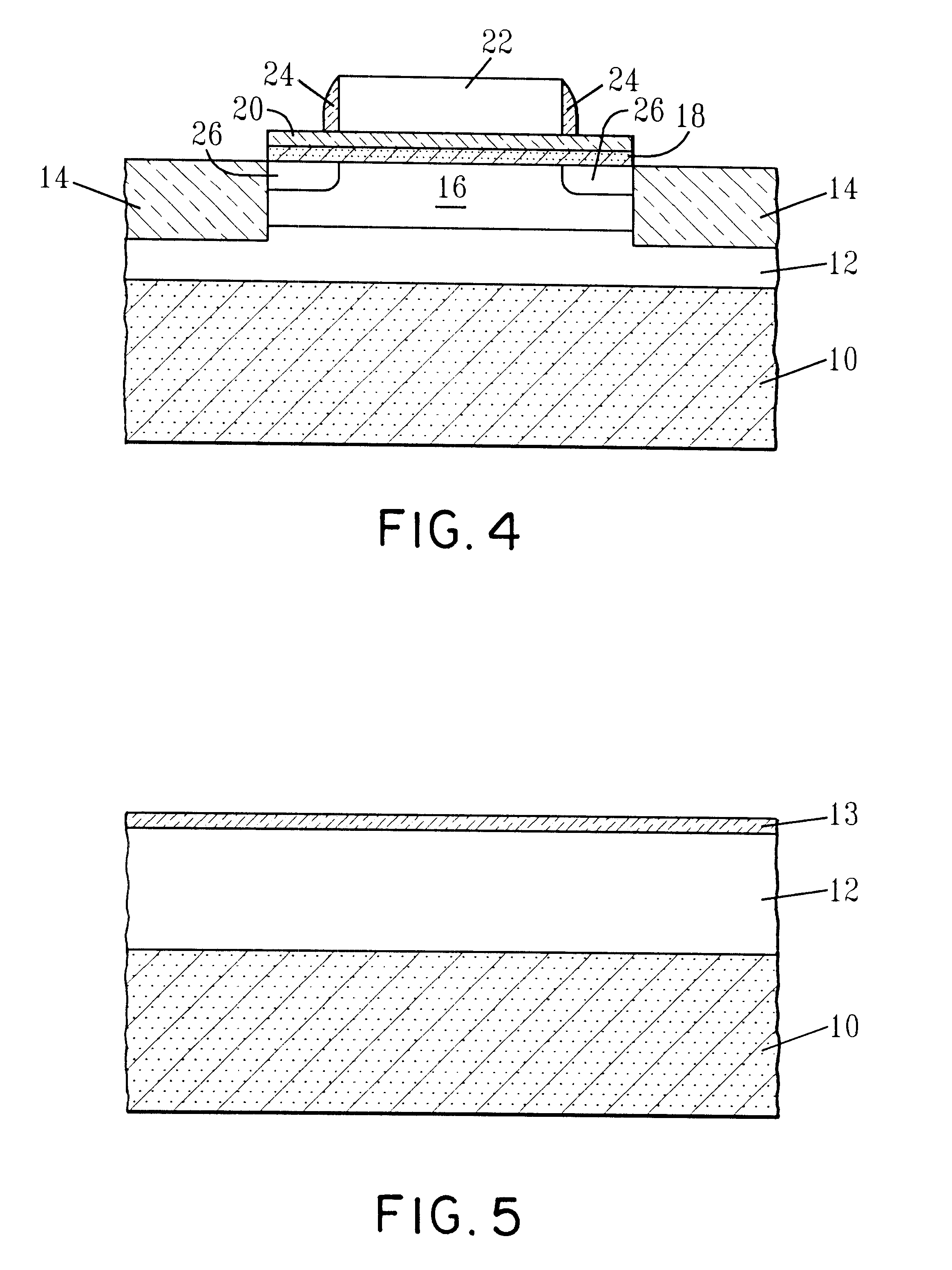
The present invention will now be described in more detail by referring to the drawings that accompany the present application. It is noted that in the accompanying drawings like reference numerals are used for describing like and / or corresponding elements.

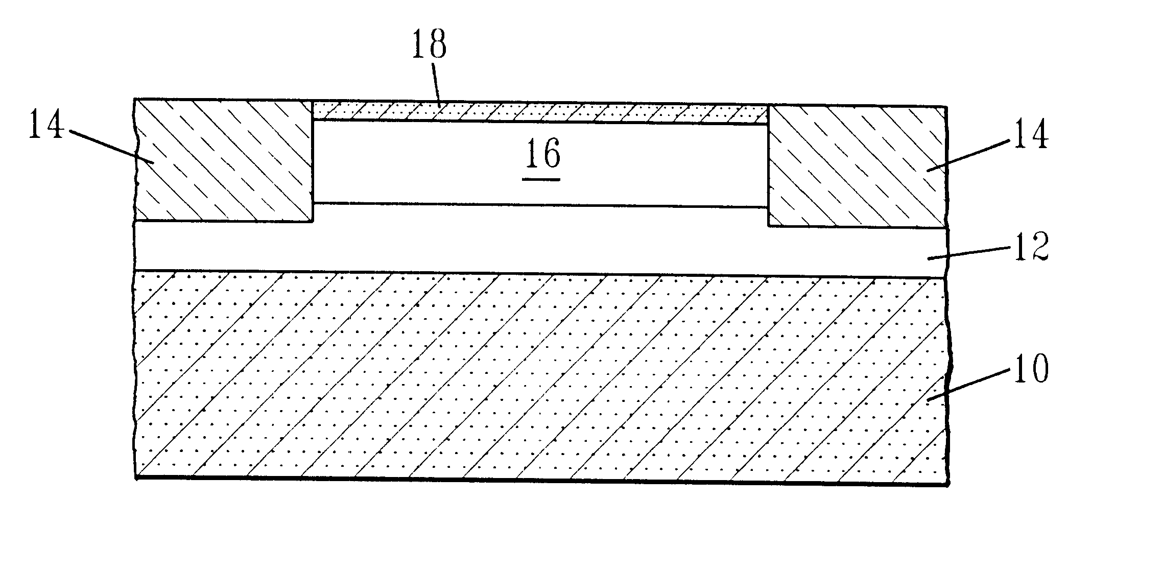
Reference is first made FIGS. 1-3 which illustrate the basic processing steps of the present invention. Specifically, FIG. 1 shows a basic structure that is formed after conducting step (a) of the present invention, i.e., after forming relaxed SiGe layer 12 on a surface of substrate 10. The relaxed SiGe layer is formed on a surface of substrate 10 utilizing any conventional process that is capable of forming such a layer on a substrate. For example, the relaxed SiGe layer may be formed utilizing a conventional growing process such as described in U.S. Pat. No. 5,158,907, a conventional Czochralski crystal pulling process, or epitaxy by solid phase regrowth such as described in U.S. Pat. No. 5,847,419; the contents of the each of t...


PUM


Abstract

A strained Si CMOS structure is formed by steps which include forming a relaxed SiGe layer on a surface of a substrate; forming isolation regions and well implant regions in said relaxed SiGe layer; and forming a strained Si layer on said relaxed SiGe layer. These processing steps may be used in conjunction with conventional gate processing steps in forming a strained MOSFET structure.

Description

FIELD OF THE INVENTIONThe present invention relates to complementary metal oxide semiconductor (CMOS) device manufacturing, and in particular to a method of forming a strained Si CMOS structure wherein the strained Si channel layer of the structure is formed after conducting various high-temperature processing steps and after conducting various processing steps that typically consume Si.BACKGROUND OF THE INVENTIONIn the semiconductor industry, `strained Si on SiGe CMOS` essentially refers to CMOS devices fabricated on a substrate that consists of a relatively thin (about 50 to about 300 .ANG.) strained Si layer epitaxially grown on top of a relatively thick (about 300 to about 20,000 .ANG.) relaxed SiGe layer. Publications in the past have shown the potential of achieving high-electron and hole mobilities in strained Si layers. More recent publications have experimentally demonstrated that strained Si layers can be used as a channel region for metal oxide field effect transistors (M...

Claims


Application Information

Patent Timeline
Patent Type & Authority Patents(United States)
IPC IPC(8): H01L21/20H01L29/02H01L21/70H01L21/02H01L21/8238H01L21/336H01L29/10H01L29/78H01L27/092H01L29/786
CPCH01L21/0237H01L21/0245H01L21/02532H01L21/02639H01L21/823807H01L21/823878H01L29/1054H01L29/66651Y10S438/933H01L21/8238
Inventor RIM, KERN
Owner SAMSUNG ELECTRONICS CO LTD
Why Eureka
Try Eureka