Programming methods for multi-level flash EEPROMS

a multi-level, flash memory technology, applied in static storage, digital storage, instruments, etc., can solve the problems of wasting valuable space in the circuitry needed to confirm that a particular cell has been properly programmed, prolonging the programming process, and requiring a substantial amount of time for verification steps, etc., to achieve fast multi-level programming of flash memory devices

Inactive Publication Date: 2005-01-18
ROUND ROCK RES LLC
View PDF36 Cites 37 Cited by
  • Summary
  • Abstract
  • Description
  • Claims
  • Application Information

AI Technical Summary

Benefits of technology

By eliminating the verification steps, the present invention achieves faster multi-level programming of flash memory devices. In accordance with one aspect of the present invention, a method is provided for programming a memory cell of an electrically erasable programmable read only memory. The memory cell is fabricated on a substrate and comprises a source region, a drain region, a floating gate, and a control gate. The memory cell has a threshold voltage selectively configurable into one of at least three programming states. The method comprises generating a drain current between the drain region and the source region by applying a drain-to-source bias voltage between the drain region and the source region. The method further comprises injecting hot electrons from the drain current to the floating gate by applying a gate voltage to the control gate. A selected threshold voltage for the memory cell corresponding to a selected one of the programming states is generated by applying a selected constant drain-to-source bias voltage.

Problems solved by technology

Such use of verification steps has two potential drawbacks.
First, the circuitry needed to confirm that a particular cell has been properly programmed takes up valuable space on the semiconductor die.
Second, the frequent verification steps take a substantial amount of time, thereby prolonging the programming process.

Method used


Image

  • Programming methods for multi-level flash EEPROMS
  • Programming methods for multi-level flash EEPROMS
  • Programming methods for multi-level flash EEPROMS

Examples


Embodiment Construction

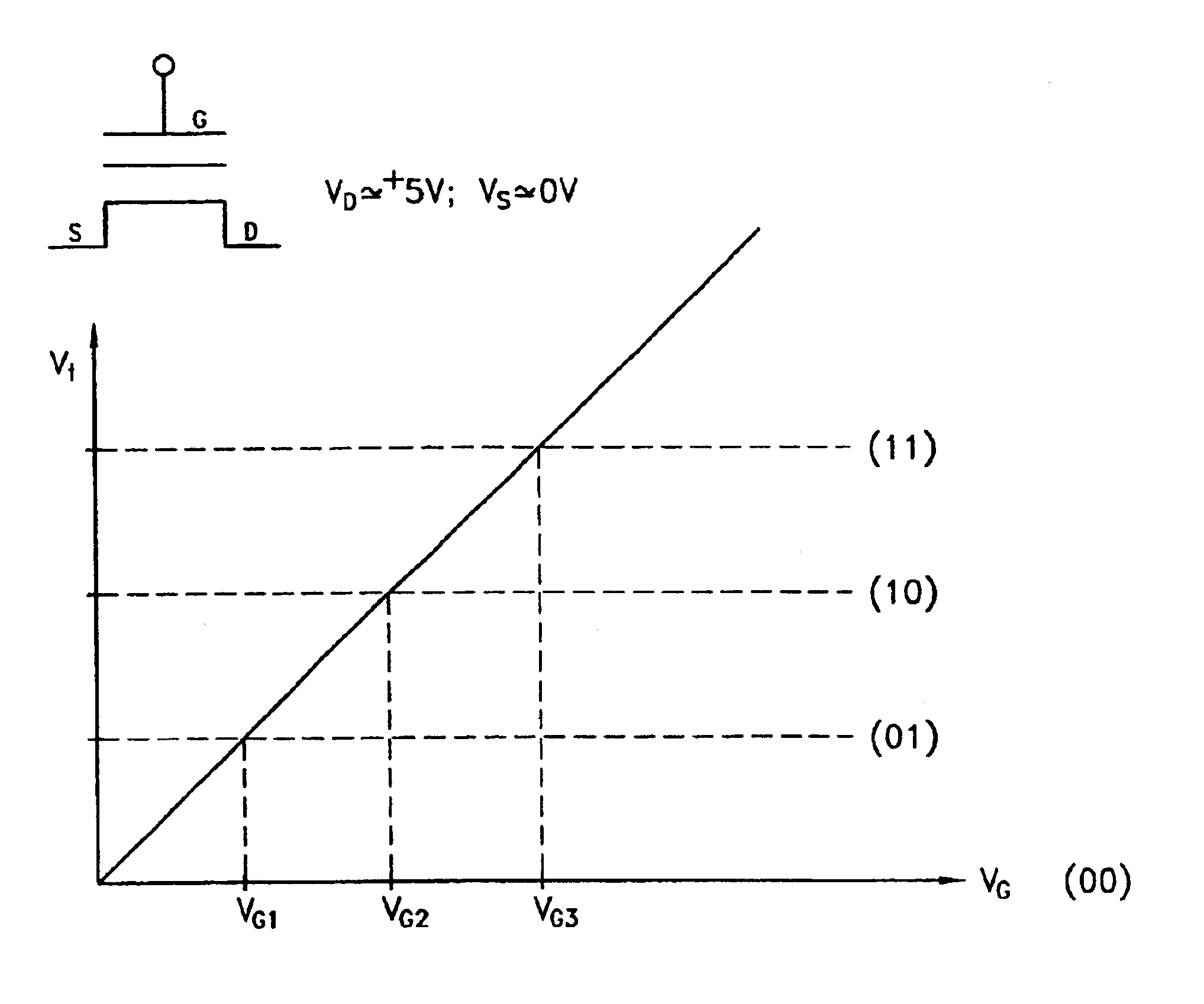
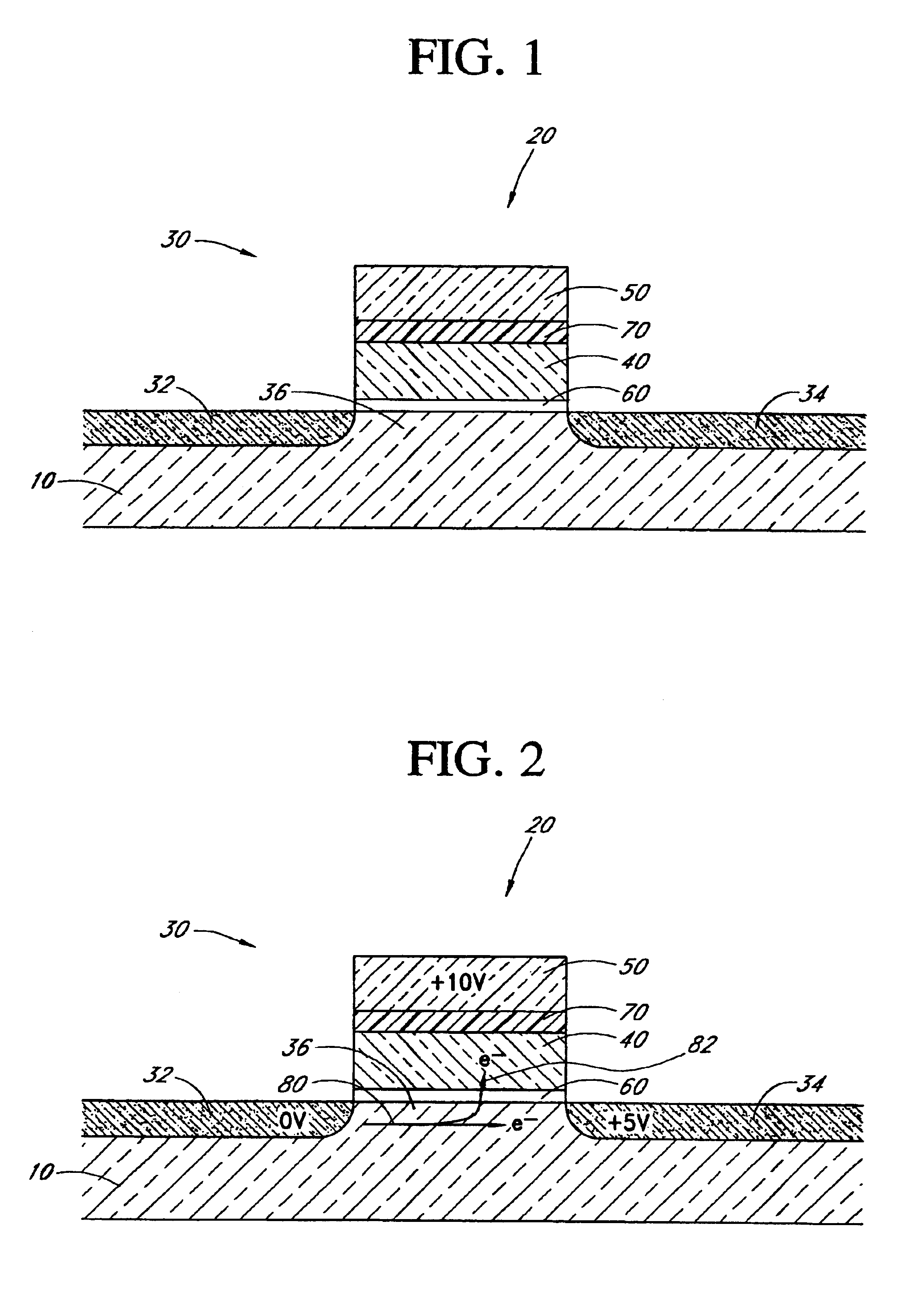
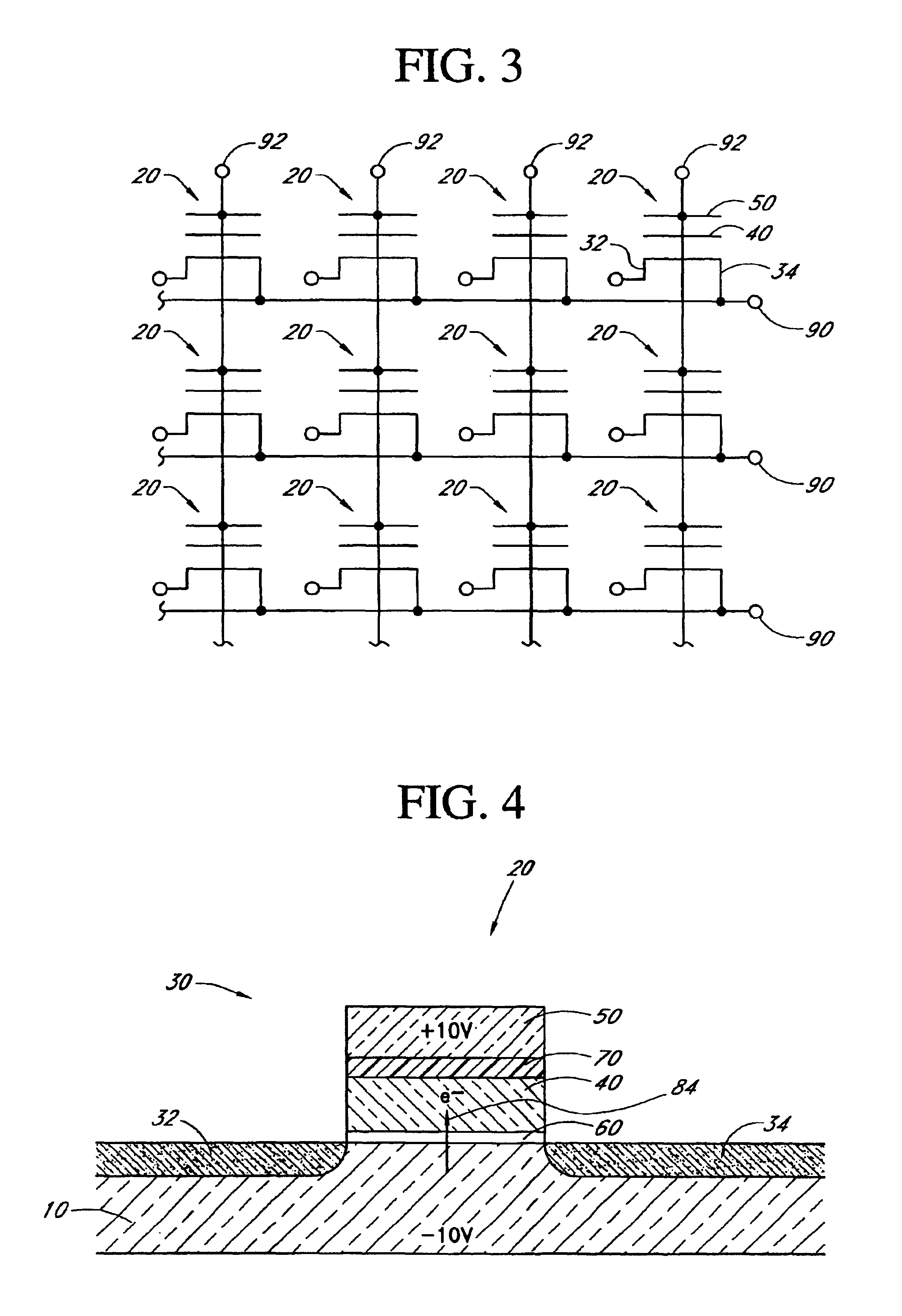
FIG. 1 schematically illustrates a semiconductor substrate 10 with a memory cell 20 compatible with the present invention. The memory cell 20 includes a transistor 30, a floating gate 40, and a control gate 50 above the floating gate 40 in a stacked gate structure. The transistor 30 comprises a source region 32, a drain region 34, and a channel 36 between the source region 32 and the drain region 34. The floating gate 40, typically composed of polycrystalline silicon (i.e., “polysilicon”), is electrically isolated from the underlying semiconductor substrate 10 by a tunnel dielectric layer 60, which is a thin dielectric layer, typically formed of an insulating oxide, and more particularly, silicon oxide, and is typically approximately 100 Å thick. The control gate 50 is positioned above the floating gate 40, and is electrically isolated from the floating gate 40 by a storage dielectric layer 70, such as oxide-nitride-oxide (ONO). Electrical access to the floating gate 40 is therefore...


PUM


Abstract

A method is provided for programming a memory cell of an electrically erasable programmable read only memory. The memory cell is fabricated on a substrate and comprises a source region, a drain region, a floating gate, and a control gate. The memory cell has a threshold voltage selectively configurable into one of at least three programming states. The method includes generating a drain current between the drain region and the source region by applying a drain-to-source bias voltage between the drain region and the source region. The method further includes injecting hot electrons from the drain current to the floating gate by applying a gate voltage to the control gate. A selected threshold voltage for the memory cell corresponding to a selected one of the programming states is generated by applying a selected constant drain-to-source bias voltage and a selected gate voltage.

Description

BACKGROUND OF THE INVENTION1. Field of the InventionThe present invention generally relates to electrically reprogrammable nonvolatile memory devices and methods of utilizing the same. More particularly, the invention relates to processes and structures for programming erasable programmable read-only memories (EEPROMs).2. Description of the Related ArtMemory devices such as erasable programmable read-only memories (EPROMs), electrically erasable programmable read-only memories (EEPROMs), or flash erasable programmable read-only memories (FEPROMs) are erasable and reusable memory cells which are often used in digital cellular phones, digital cameras, LAN switches, cards for notebook computers, etc. A memory cell operates by storing electric charge (representing either a binary “1” or “0” state of one data bit) on an electrically isolated floating gate, which is incorporated into a transistor. This stored charge affects the threshold voltage (VT) of the transistor, thereby providing a...

Claims


Application Information

Patent Timeline
Patent Type & Authority Patents(United States)
IPC IPC(8): G11C7/00G11C16/04G11C11/34G11C11/56
CPCG11C16/0483G11C11/5628
Inventor CHEN, CHUNPRALL, KIRK D.
Owner ROUND ROCK RES LLC
Why Eureka
Try Eureka