Area array semiconductor package and 3-dimensional stack thereof

a technology of semiconductor packages and stacked devices, applied in semiconductor devices, semiconductor/solid-state device details, electrical devices, etc., can solve the problems of reducing reliability and yield, reducing the productivity of the assembly process, and requiring good chips to be discarded along with the failing chip, so as to improve the interconnection of the packag

Inactive Publication Date: 2005-01-25
SAMSUNG ELECTRONICS CO LTD
View PDF15 Cites 152 Cited by
  • Summary
  • Abstract
  • Description
  • Claims
  • Application Information

AI Technical Summary

Problems solved by technology

The use of several chips in a single package does, however, tend to reduce both reliability and yield.
If, during post assembly testing, just one chip in the multi-chip or chip stack package fails to meet the functional or performance specifications, the entire package fails, causing the good chip(s) to be discarded along with the failing chip.
As a result, multi-chip and chip stack package tend to lower the productivity from the assembly process.

Method used


Image

  • Area array semiconductor package and 3-dimensional stack thereof
  • Area array semiconductor package and 3-dimensional stack thereof
  • Area array semiconductor package and 3-dimensional stack thereof

Examples


Embodiment Construction

Exemplary embodiments of the invention will be described below with reference to accompanying drawings. This invention may, however, be embodied in many different forms and should not be construed as being limited to the exemplary embodiments set forth herein; rather, these exemplary embodiments are provided so that this disclosure is thorough and complete, and conveys the concept of the invention to those skilled in the art. In the drawings, the thickness and spacing of layers and regions may be enlarged or reduced for clarity and are not intended to be to scale. When a layer is referred to as being “on” another layer or substrate, the layer may be directly on the other layer or substrate, or intervening layers may also be present.

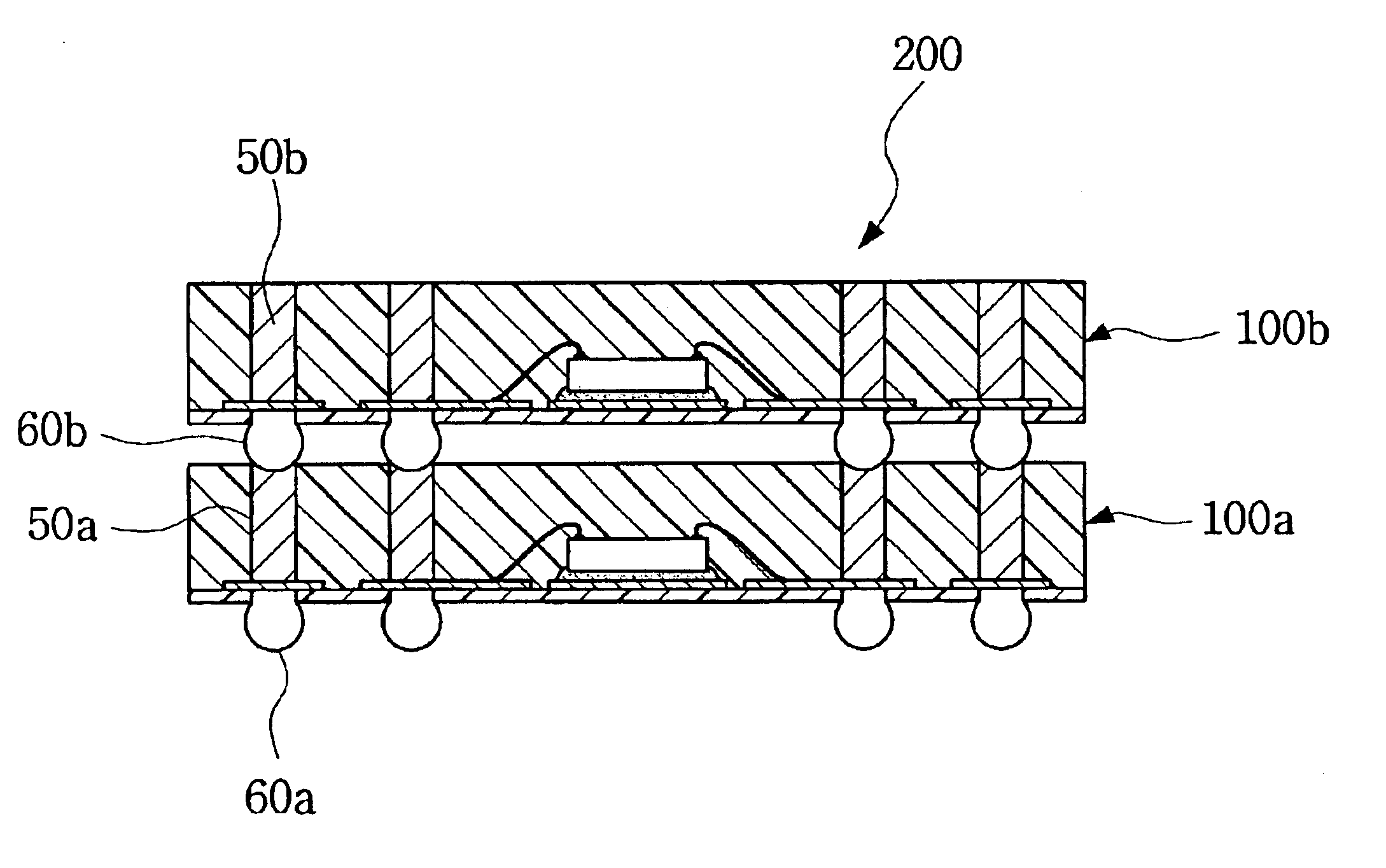
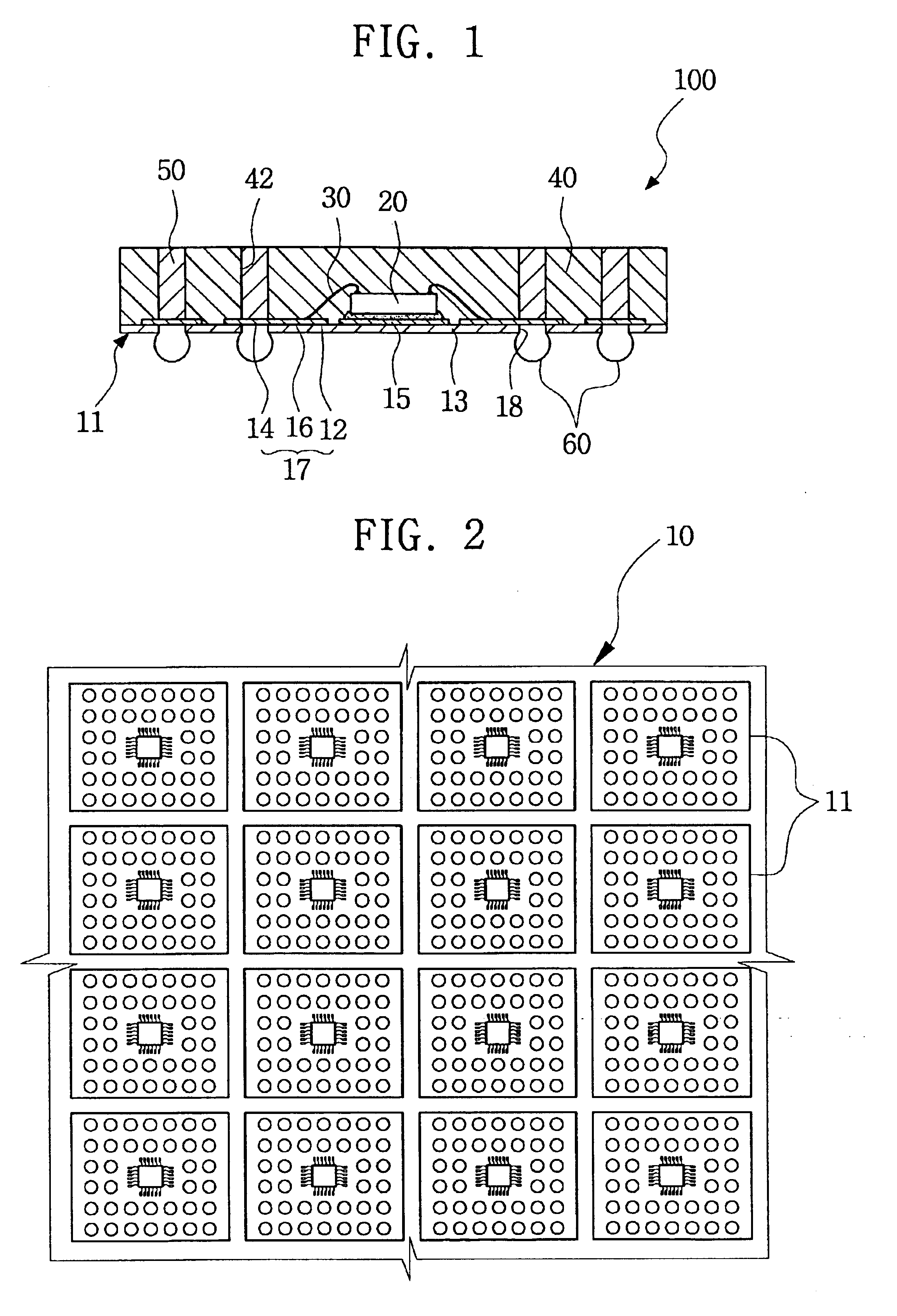
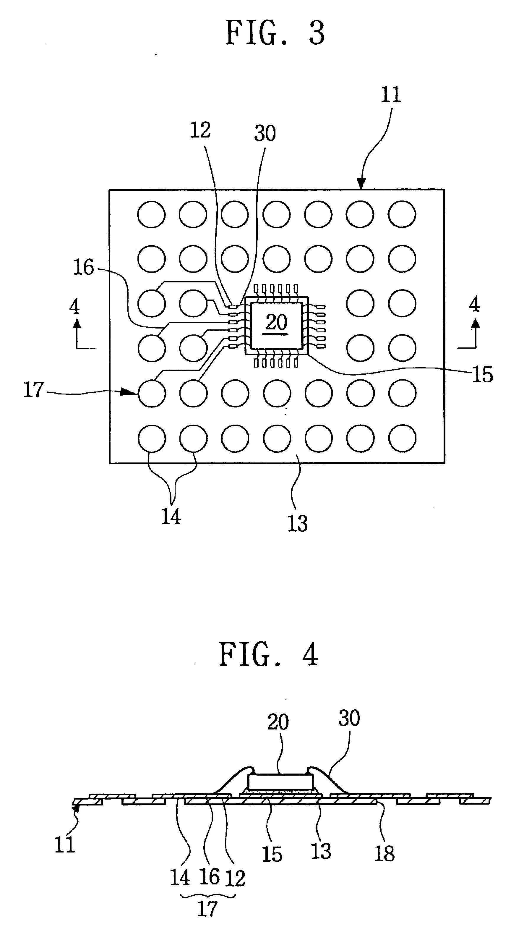
FIG. 1 is a cross-sectional view of an exemplary embodiment of the invention showing an area array type semiconductor package 100. Referring to FIG. 1, a plurality of solder balls 60 may be formed on the lower surface of semiconductor package 100, with a ...


PUM


Abstract

An area array type semiconductor package suitable for use in the formation of a 3-dimensional stack of the area array type packages. The area array type semiconductor package includes a circuit board, typically a tape circuit board, a semiconductor chip, bonding wires, an encapsulation body, solder posts, and solder balls. A plurality of the area array type semiconductor packages can be electrically connected through the corresponding solder balls and solder posts on adjacent packages to form semiconductor stack packages.

Description

BACKGROUND OF THE INVENTIONThis U.S. nonprovisional patent application claims priority under 35 U.S.C. § 119 of Korean Patent Application 2002-58056 filed on Sep. 25, 2002, the entire contents of which are hereby incorporated by reference.1. Field of the InventionThe present invention generally relates to semiconductor package assembly technology and, more particularly, to an area array type semiconductor package and 3-dimensional stack of area array type packages.2. Description of the Prior ArtThe electronic industry continues to seek products that are lighter, faster, smaller, multi-functional, more reliable and more cost-effective. In an effort to meet such requirements, package assembly techniques have been developed for multi-chip packages (MCP) and chip stack packages. These types of packages combine two or more semiconductor chips in a single package, thereby realizing increased memory density, multi-functionality and / or reduced package footprint.The use of several chips in a...

Claims


Application Information

Patent Timeline
Patent Type & Authority Patents(United States)
IPC IPC(8): H01L21/02H01L21/44H01L23/48H01L23/28H01L21/56H01L23/31H01L23/538H01L25/10
CPCH01L21/561H01L23/5384H01L23/5387H01L23/5389H01L24/97H01L25/105H01L23/3128H01L2225/1058H01L2224/48091H01L2224/48227H01L2224/48465H01L2224/73265H01L2224/97H01L2924/01079H01L2924/01082H01L2924/15311H01L2924/15331H01L2225/1023H01L2924/01033H01L2924/01006H01L24/48H01L2224/49175H01L2224/32225H01L2224/85H01L2224/83H01L2924/00014H01L2924/00H01L24/49H01L2224/05599H01L2224/45099H01L2224/85399H01L2924/12042H01L2924/181H01L2924/00012H01L2224/45015H01L2924/207H01L23/28
Inventor SHIM, JONG BO
Owner SAMSUNG ELECTRONICS CO LTD
Why Eureka
Try Eureka