Programmably disabling one or more cache entries
- Summary
- Abstract
- Description
- Claims
- Application Information
AI Technical Summary
Benefits of technology
Problems solved by technology
Method used
Image
Examples
Embodiment Construction
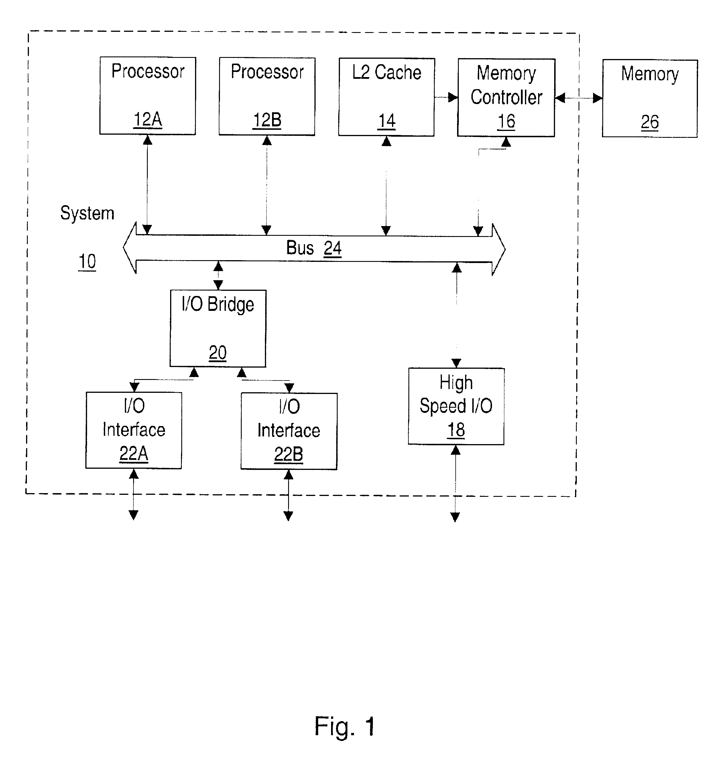
Turning now to FIG. 1, a block diagram of one embodiment of a system 10 is shown. Other embodiments are possible and contemplated. In the embodiment of FIG. 1, system 10 includes processors 12A-12B, an L2 cache 14, a memory controller 16, a high speed input / output (I / O) interface 18, an I / O bridge 20, and I / O interfaces 22A-22B. System 10 may include a bus 24 for interconnecting the various components of system 10. As illustrated in FIG. 1, each of processors 12A-12B, L2 cache 14, memory controller 16, high speed I / O interface 18 and I / O bridge 20 are coupled to bus 24. I / O bridge 20 is coupled to I / O interfaces 22A-22B. L2 cache 14 is coupled to memory controller 16, which is further coupled to a memory 26.
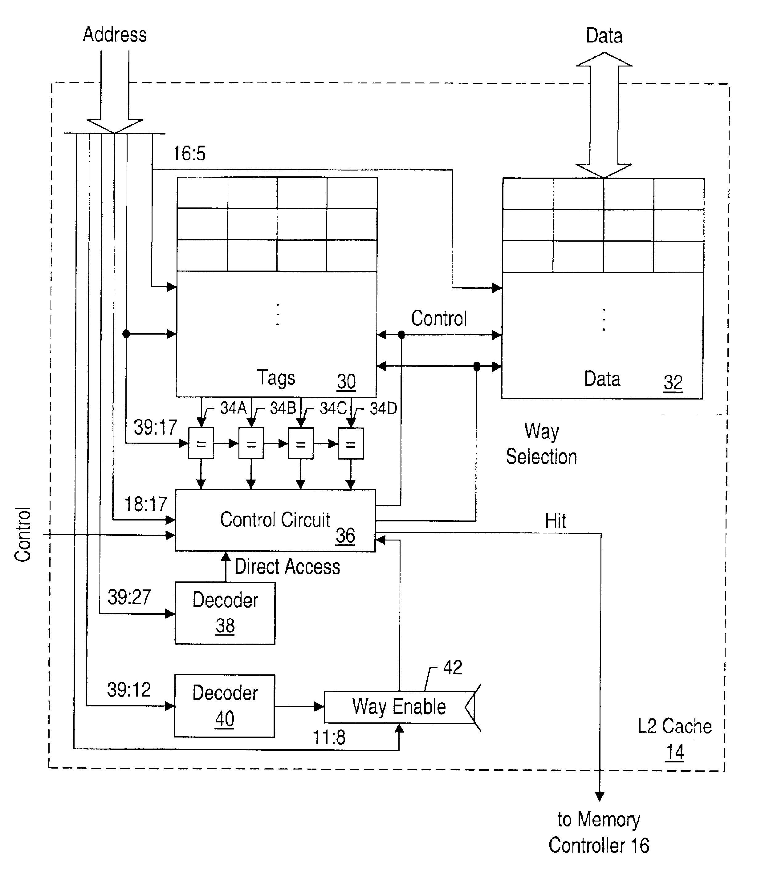
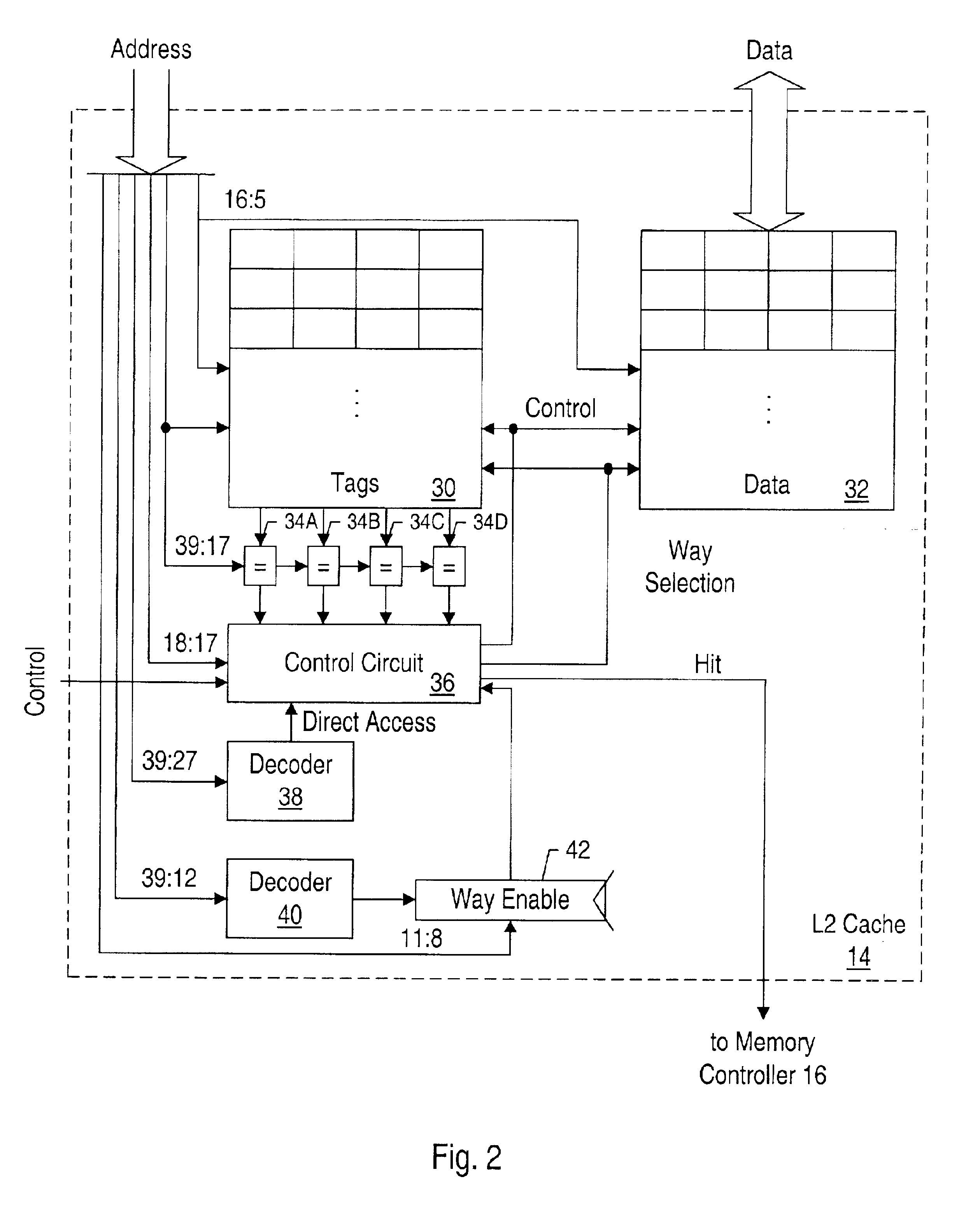
Generally, L2 cache 14 may support the programmable disabling of one or more entries from allocation in response to memory transactions which miss L2 cache 14. Furthermore, L2 cache 14 may support the selection of which of the cache entries are disabled. For example, L2 cache 14 ...
PUM
 Abstract
Description
Claims
Application Information


