Laser programmable electrically readable phase-change memory method and device

a phase-change memory and phase-change technology, applied in the field of non-volatile, high density, integrated circuit memory devices, can solve the problems of complex structures that can affect the reliability of memory devices, difficult to provide a source/drain current of more than 1 ma for a minimum size device, etc., to achieve the effect of simple electrical circuit, low power consumption, and not requiring slow and power-

Inactive Publication Date: 2005-02-01
MACRONIX INT CO LTD
View PDF17 Cites 274 Cited by
  • Summary
  • Abstract
  • Description
  • Claims
  • Application Information

AI Technical Summary

Benefits of technology

According to the invention, roughly described, a chalcogenide-based memory is programmed optically and read electrically. No complex electrical circuits are required for programming the cells. On the other hand, this memory can be read by electrical circuitry directly. The read out speed is much faster than for optical disks, and integrated circuit chips mad

Problems solved by technology

In a standard MOS IC, it is very difficult to provide a source/drain current of more than 1 mA for a minimum size device.
In addition, even if such feats were possible, the high power consumed would be very undesirable for many applications.
Furthermore, complex structures can affect the reliability of the memory devices.
Large cell sizes

Method used


Image

  • Laser programmable electrically readable phase-change memory method and device
  • Laser programmable electrically readable phase-change memory method and device
  • Laser programmable electrically readable phase-change memory method and device

Examples


Embodiment Construction

The following detailed description is made with reference to the figures. Preferred embodiments are described to illustrate the present invention, not to limit its scope, which is defined by the claims. Those of ordinary skill in the art will recognize a variety of equivalent variations on the description that follows.

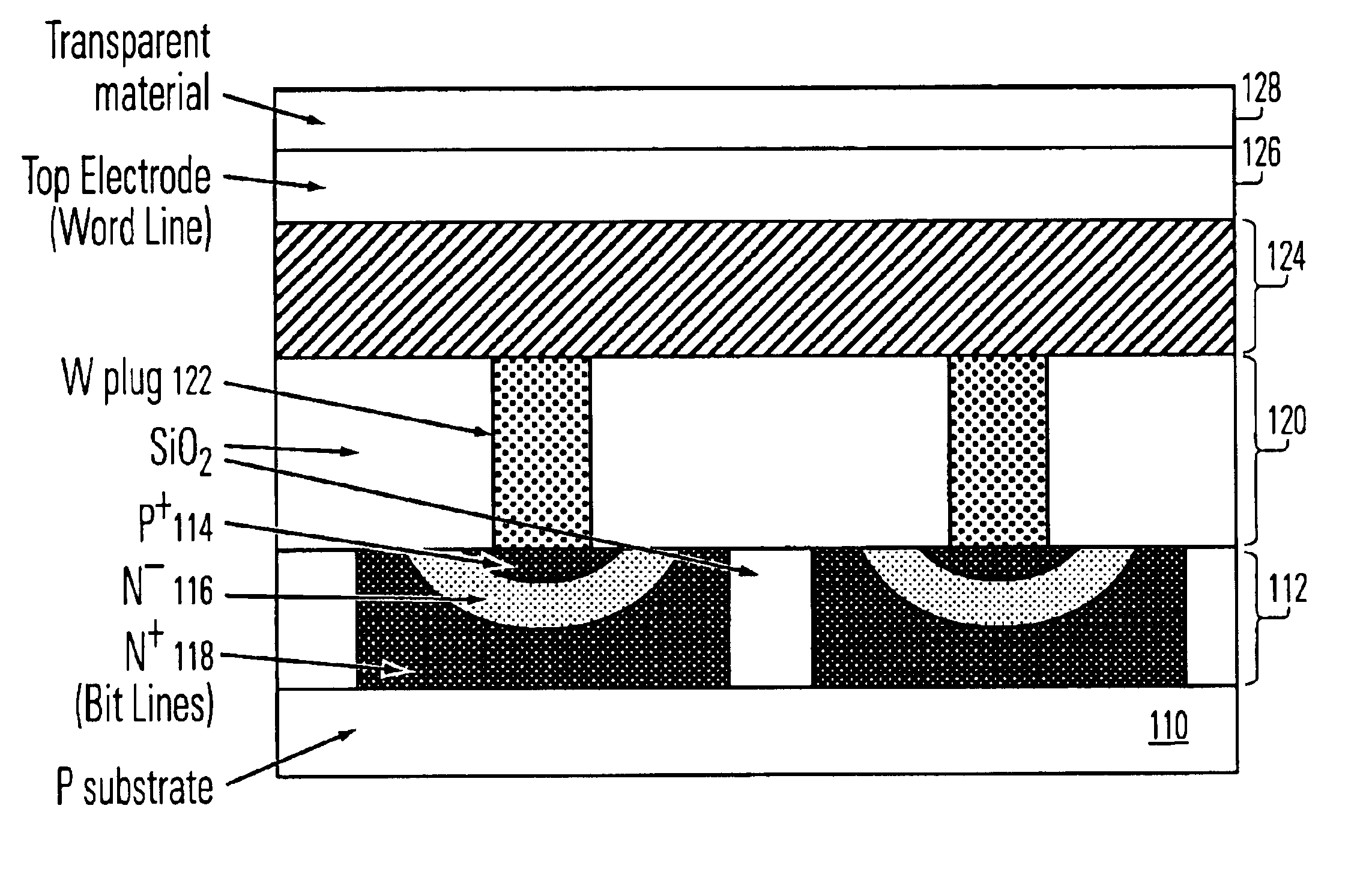
A chalcogenide material contains one or more elements from column six of the periodic table of elements. Many chalcogenide phase-change alloys have been described in technical literature, including alloys of: Ga / Sb, In / Sb, In / Se, Sb / Te, Ge / Te, Ge / Sb / Te, In / Sb / Te, Ga / Se / Te, Sn / Sb / Te, In / Sb / Ge, Ag / In / Sb / Te, Ge / Sn / Sb / Te, Ge / Sb / Se / Te and Te / Ge / Sb / S. In the family of Ge / Sb / Te alloys, a wide range of alloy compositions may be workable. The compositions can be characterized as TeaGebSb100−(a+b). One researcher has described the most useful alloys as having an average concentration of Te in the deposited materials well below 70%, typically below about 60% and ranged in general...


PUM


Abstract

Roughly described, a phase-change memory such as a chalcogenide-based memory is programmed optically and read electrically. No complex electrical circuits are required for programming the cells. On the other hand, this memory can be read by electrical circuitry directly. The read out speed is much faster than for optical disks, and integrated circuit chips made this way are more compatible with other electrical circuits than are optical disks. Thus memories according to the invention can have simple, low power-consuming, electrical circuits, and do not require slow and power-hungry disk drives for reading. The invention therefore provides a unique low power, fast read/write memory with simple electrical circuits.

Description

BACKGROUNDField of the InventionThe present invention relates to non-volatile, high density, integrated circuit memory devices, and more particularly to such memory devices based upon phase change materials such as chalcogenides.ReferencesThe following documents are incorporated by reference herein: U.S. Pat. Nos. 5,837,564; 3,530,441; 4,912,066; 4,455,495; 4,719,594; 5,789,758; 6,077,729; 6,153,890; RE37,259; 5,687,112; 5,789,277; 6,185,122 and 6,150,253. PCT publication PCT / US00 / 33562. Noboru Yamada, “Potential of Ge—Sb—Te Phase-Change Optical Disks for High-Data-Rate Recording”, SPIE v.3109, pp. 28-37 (1997).Description of Related ArtChalcogenides have been utilized in the formation of memory cells for integrated circuit memory devices. Representative prior art patents in this field include Reinberg U.S. Pat. No. 5,789,758, Harshfield U.S. Pat. No. 6,077,729, Wolstenholme U.S. Pat. No. 6,153,890, Ovshinsky U.S. Reissue Pat. No. RE37,259 (Reissue of U.S. Pat. No. 5,687,112), Zahor...

Claims


Application Information

Patent Timeline
IPC IPC(8): G11C16/18G11C16/02G11C16/06G11C16/10
CPCG11C13/0004G11C16/18G11C2213/72G11C13/04
Inventor LU, CHIH-YUANCHEN, YI-CHOU
Owner MACRONIX INT CO LTD
Why Eureka
Try Eureka