Close packing LED assembly with versatile interconnect architecture

a technology of interconnection and closed packing, applied in the field of electronic and optoelectronic arts, can solve the problems of limited application range, limited choice of substrate, and substrates which are used for the growth of such layers

Inactive Publication Date: 2005-02-08
GELCORE LLC (US)
View PDF11 Cites 123 Cited by
  • Summary
  • Abstract
  • Description
  • Claims
  • Application Information

AI Technical Summary

Problems solved by technology

This approach is limited in application.
The choice of substrate is limited to those compatible with the semiconductor layer generation method.
Many commercial LEDs are formed from III-V compound semiconductor layers, and the substrates which are used for the growth of such layers, typically including GaAs and InP wafers, sapphire substrates, and the like, are often expensive, fragile, and of limited lateral area.
However, the individual LEDs are electrically isolated, so that intricate wire bonding or other electrical interconnecting methods are typically applied to complete the array.
Additionally, a different host substrate shape and electrical interconnect pattern is needed for each distinct LED arrangement, which limits the standardization of parts and complicates array manufacturing.

Method used


Image

  • Close packing LED assembly with versatile interconnect architecture
  • Close packing LED assembly with versatile interconnect architecture
  • Close packing LED assembly with versatile interconnect architecture

Examples


Embodiment Construction

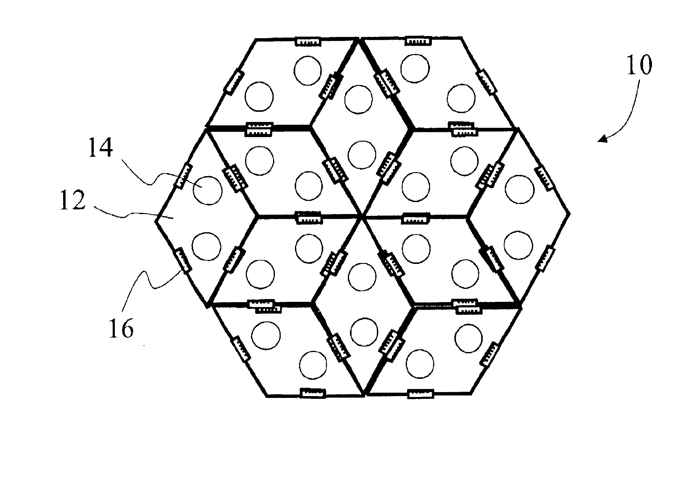
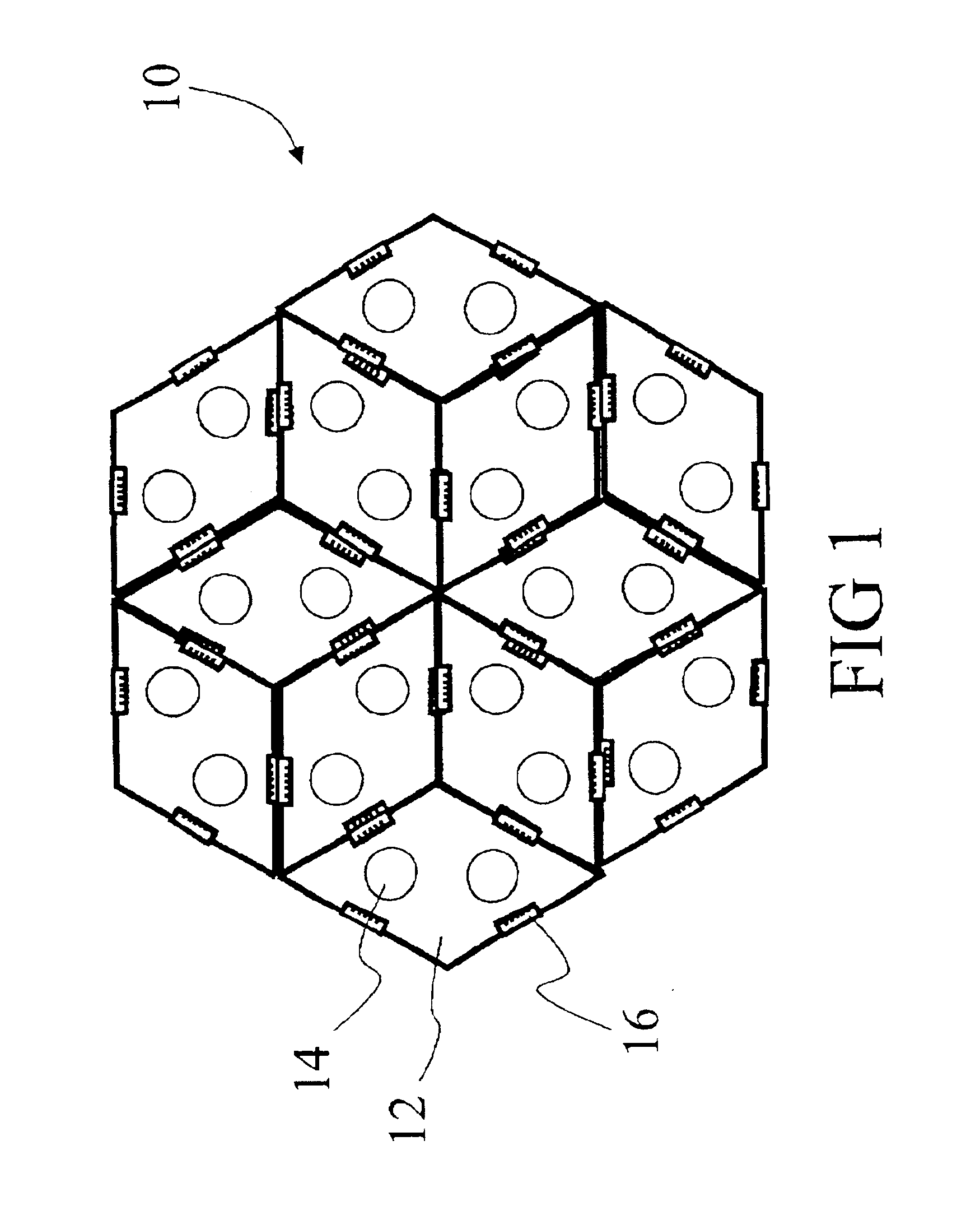
With reference to FIGS. 1 and 2, a modular mounting assembly 10 is described. A plurality of substrates 12 each have one or more components 14 arranged thereon. In the illustrated embodiment of FIG. 7, each substrate 12 has two LED components 14 arranged thereon. The plurality of substrates 12 are arranged in a selected manner to form the mounting assembly 10 that arranges the components 14 in a selected arrangement, such as the hexagonal arrangement of FIG. 1 comprised of twelve substrates 12 and twenty four LED components 14.

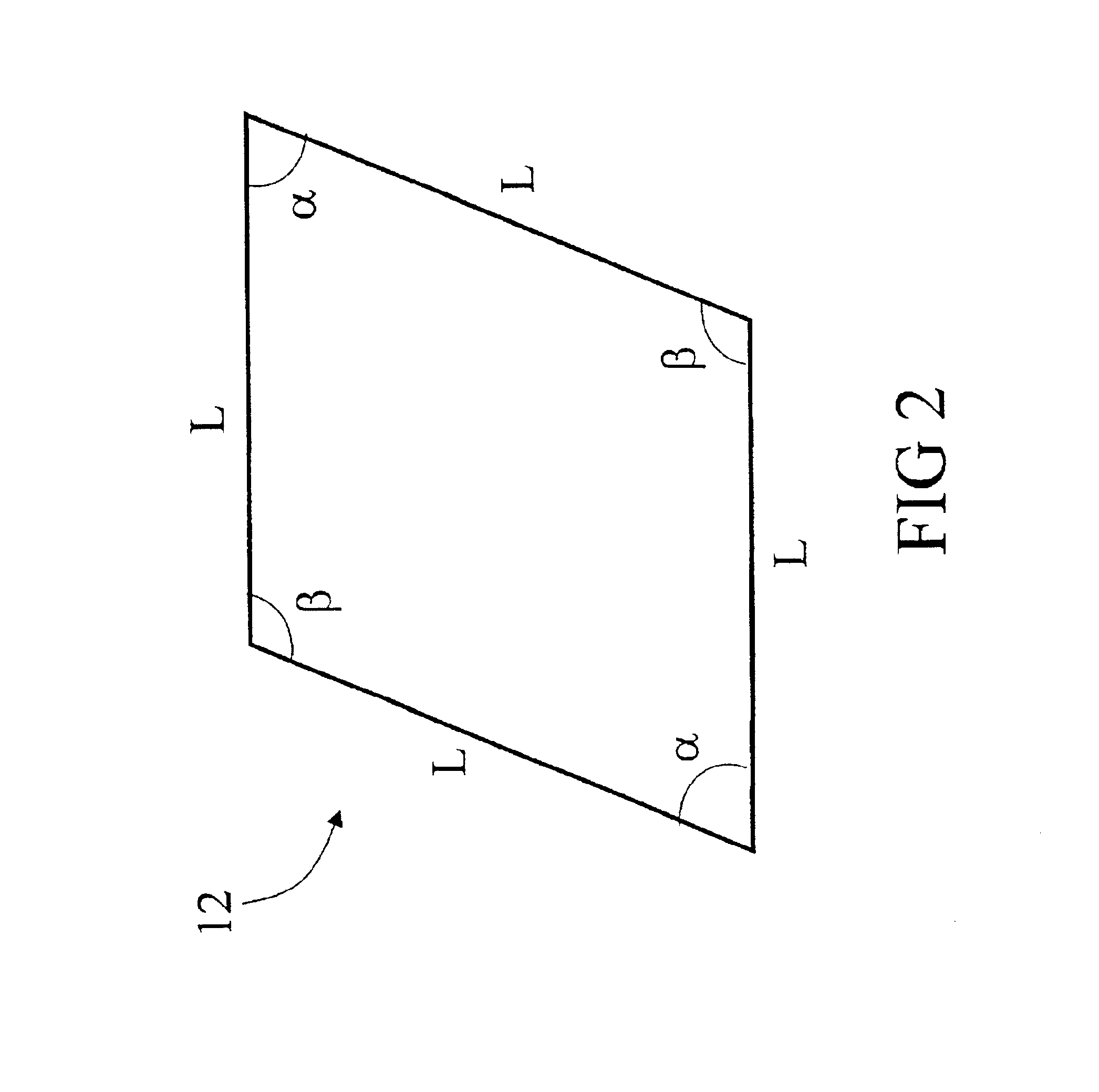
In one embodiment shown in FIGS. 1 and 2, each substrate 12 has the shape of a rhombus, i.e. a parallelogram having four sides of essentially equal length L, with oppositely oriented angles equal. Thus, a rhombus can be specified by two angular parameters α and β, along with the side length L, as shown in FIG. 2. In the illustrated embodiment of FIG. 1, the angles α and β are 60° and 120°, respectively, so that each rhombic substrate 12 corresponds to a primit...


PUM


Abstract

A modular mounting assembly (10) for connecting a plurality of LEDs in a selectable electrical and spatial arrangement includes a plurality of substrates (12) each having at least one LED (14a, 14b) fixedly arranged thereon, and a plurality of connectors (16) arranged thereon that are in operative communication with the at least one LED (14a, 14b) fixedly arranged thereon. The plurality of substrates (12) are arranged in a selected spatial arrangement having selected pairs of connectors (16) in operative communication with each other to effectuate electrical connection therebetween, whereby an electrical arrangement of the plurality of LEDs is effectuated. A plurality of interconnecting elements (50A, 50D, 50S, 50P) electrically and structurally interconnect selected spatially adjacent substrates (12) in cooperation with the selected pairs of connectors. A connector (16) has a plurality of electrical conductor members (1, 2, 3, 4, 5), and an interconnecting element (50) has a selected electrical configuration that effectuates a selected interconnection of conductor members (1, 2, 3, 4, 5).

Description

BACKGROUND OF INVENTIONThe invention relates to the electronic and optoelectronic arts. It is especially applicable to the packaging of light emitting diodes (LEDs) and will be described with particular reference thereto. However, the invention will also find application in the packaging other electronic and optoelectronic devices, such as photodetectors, signal receivers, vertical cavity surface emitting lasers (VCSELs), photovoltaic devices, and the like.Light emitting diodes find application in fiber optical communications, lighting applications, display applications, and other applications where a compact, low voltage, rugged, and high efficiency light source is advantageous. In many LED applications, a plurality of LEDs are advantageously arranged into an array or other pre-determined arrangement comprising similar or dissimilar LED types. In lighting or display applications, LEDs emitting in the red, green, and blue regions are preferably closely packed to form a color “pixel”...

Claims


Application Information

Patent Timeline
Patent Type & Authority Patents(United States)
IPC IPC(8): H01R29/00H05K1/14
CPCH01R29/00F21S2/005F21V23/06H05K1/142F21S4/001Y10S362/80H01R12/52F21Y2101/02F21Y2113/005F21S4/10F21Y2115/10F21Y2113/13
Inventor KARLICEK, JR., ROBERT F.
Owner GELCORE LLC (US)
Why Eureka
Try Eureka