Input/output circuit, reference-voltage generating circuit, and semiconductor integrated circuit

a reference-voltage generating circuit and input/output technology, applied in the direction of transmission, transmission line coupling arrangement, amplifier input/output impedence modification, etc., can solve the problem of mismatch between the reference voltage from the reference-voltage source and the logical threshold value, timing errors such as clock duty errors and clock skews

Inactive Publication Date: 2005-02-08
LONGITUDE LICENSING LTD
View PDF6 Cites 37 Cited by
  • Summary
  • Abstract
  • Description
  • Claims
  • Application Information

AI Technical Summary

Benefits of technology

According to the present invention, the foregoing object is attained by providing an input / output circuit in which an output circuit, which includes at least a series circuit comprising a transistor and a resistor between an input / output pin and a power supply, has means for turning on the transistor at the time of a signal input, thereby causing the series circuit to operate as a terminating circuit of a line connected to the input / output pin.

Problems solved by technology

Further, in the conventional circuit, the transmitted signal in the output circuit is reflected again owing to mismatch of impedance with respect to the signal source of the line.
However, in the conventional circuit in which the reference voltage is supplied from a reference-voltage source exterior to the chip, a mismatch occurs between the reference voltage from the reference-voltage source and the logical threshold value when there is a discrepancy in the logical threshold value owing to a difference from one chip to another owing to the manufacturing process.
As a consequence, there is a shift in the timing at which a signal is input to the internal circuit from the input circuit, and timing error such as clock duty error and clock skew can occur.

Method used


Image

  • Input/output circuit, reference-voltage generating circuit, and semiconductor integrated circuit
  • Input/output circuit, reference-voltage generating circuit, and semiconductor integrated circuit
  • Input/output circuit, reference-voltage generating circuit, and semiconductor integrated circuit

Examples


first embodiment

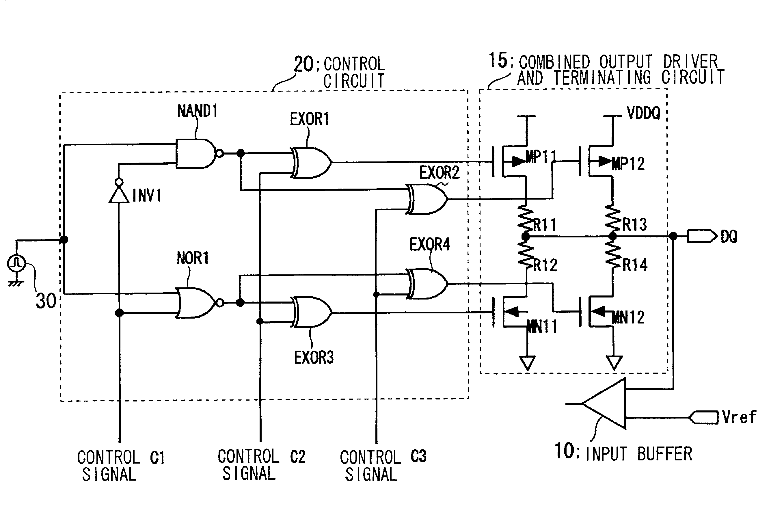
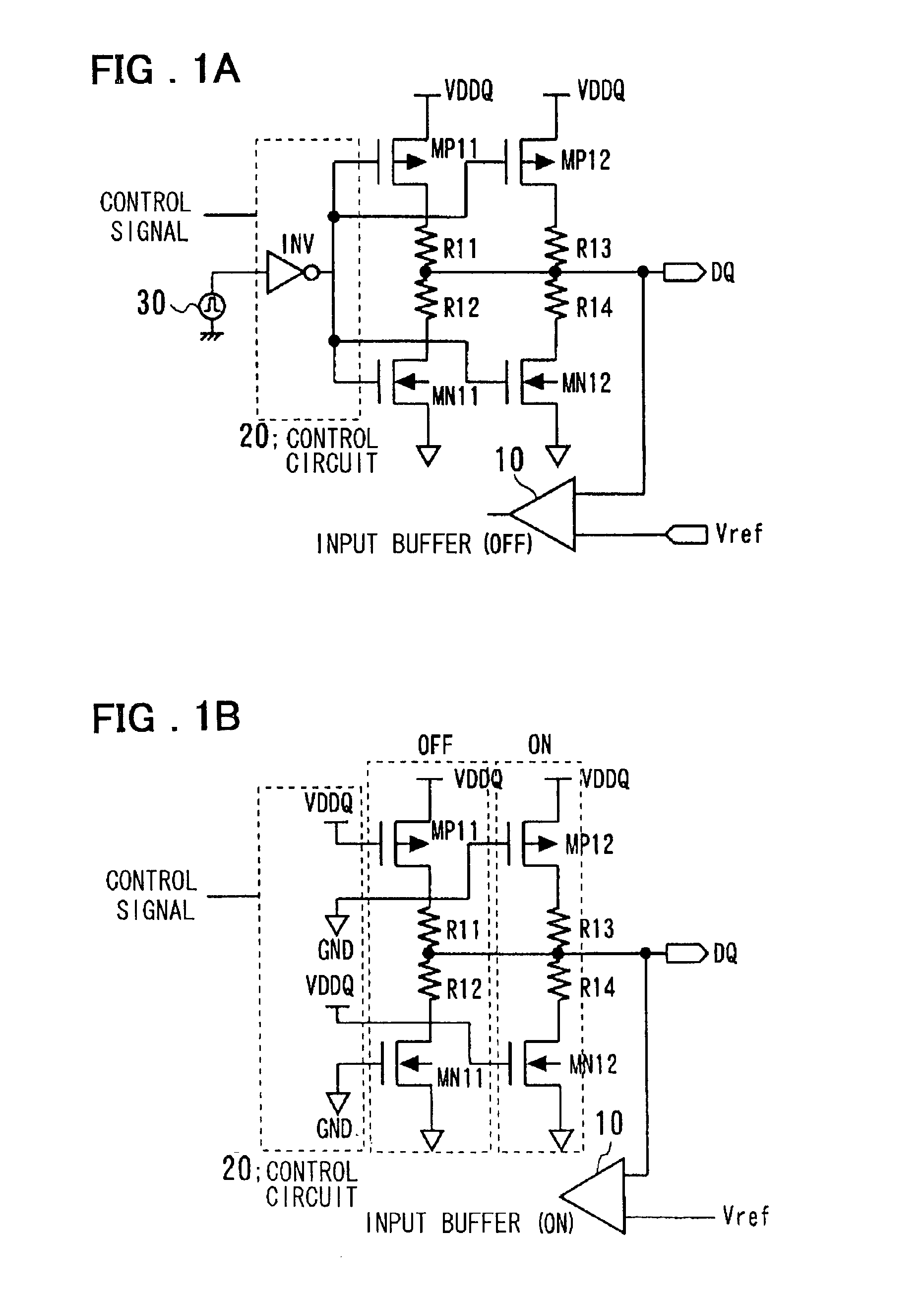
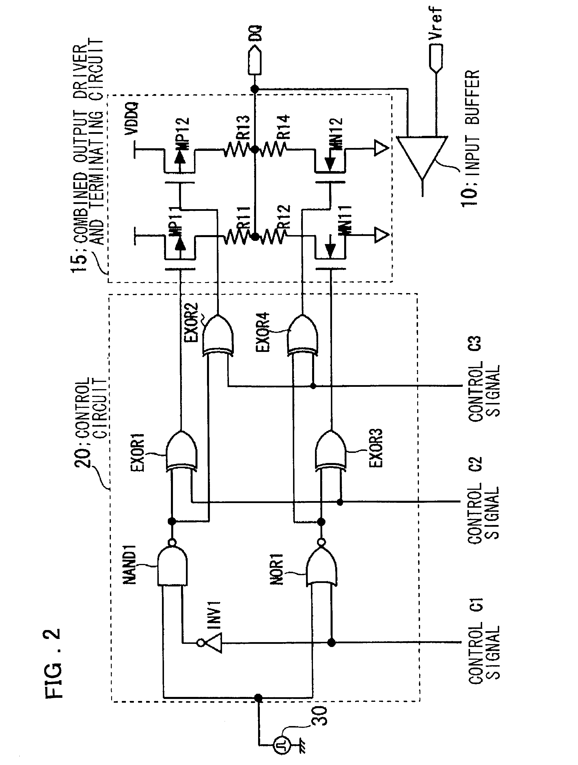
FIGS. 1A and 1B are circuit diagrams useful in describing the present invention, in which FIG. 1A illustrates the circuit connections at the time of signal transmission from the input / output circuit (i.e., in the output mode) and FIG. 1B the circuit connections at the time of signal reception (i.e., in the input mode). The output and input modes are decided by a command from a host device (not shown), and a control signal for controlling input / output is set to a logical value that is in accordance with the output or input mode. The method of generating the control signal is not directly related to the gist of the present invention and need not be described.

Referring to FIG. 1A, data from a data source 30 and a control signal for controlling input / output are supplied to a control circuit 20. When the control signal is indicative of the output mode, the control circuit 20 outputs a signal obtained on inverting the data by an inverter INV. The input / output circuit includes P-channel MO...

sixth embodiment

A memory device according to the present invention will now be described.

FIGS. 8A and 8B are diagrams illustrating an example of a memory device according to a sixth embodiment of the present invention. Specifically, an example of a point-to-point memory bus interface is illustrated, in which FIG. 8A is a perspective view illustrating components mounted on a printed circuit board, and FIG. 8B a sectional view illustrating a cross section of the memory bus (signal wiring) of the circuit board, the section being taken along line X-X′ in FIG. 8A.

Referring to FIG. 8A, the memory device includes a printed circuit board 300, a memory controller 330 mounted on the printed circuit board 300, first and second connectors 340 and 350 mounted on the printed circuit board 300, and first and second memory modules 310 and 320 inserted into the first and second connectors 340, and 350, respectively. A plurality of DRAMs (dynamic random-access memories) 311, 321 are mounted on the memory modules 310...


PUM


Abstract

Disclosed is an input / output circuit having a terminating circuit that contributes to a smaller chip area. The input / output includes an output buffer having a first series circuit, which comprises a first transistor and a resistor and a second series circuit, which comprises a second transistor and a resistor, connected in parallel between a high-potential power supply and an input / output pin, as well as a third series circuit, which comprises a third transistor and a resistor and a fourth series circuit, which comprises a fourth transistor and a resistor, connected in parallel between the input / output pin and a low-potential power supply. The input / output circuit further includes an input buffer having an input terminal connected to the input / output pin, and a control circuit which, at the time of a signal output, performs control for supplying a signal, which is obtained by inverting the logic of output data, to gates of the first to fourth transistors, and which, at the time of a signal input, performs control for supplying the gates of the first and third transistors with the high-potential power supply voltage and low-potential power supply voltage, respectively, and the gates of the second and fourth transistors with the low-potential power supply voltage and high-potential power supply voltage, respectively.

Description

FIELD OF THE INVENTIONThis invention relates to a bi-directional input / output interface for a signal input and output and, more particularly, to a termination of a transmission line and to a reference-voltage generating circuit.BACKGROUND OF THE INVENTIONIn a high-speed logic circuit in which signal rise and fall times are short, there are instances where it becomes necessary to treat a signal line as a transmission line of a distributed-constant circuit. For example, reflection must be taken into account when the propagation delay time of a transmission line is large in comparison with the rise and fall times of the output signal. That is, when a circuit having impedance different from the characteristic impedance of a transmission line is connected to the transmission line, reflection is produced at the point of connection. As is well known, a reflection coefficient ρ1 at the receiving end is given by the following equation:ρ1=(ZL−Z0) / (ZL+Z0)where Z0 represents the characteristic ...

Claims


Application Information

Patent Timeline
Patent Type & Authority Patents(United States)
IPC IPC(8): H03K19/0185H04L25/02H03K19/0175H03F1/56H03F3/62
CPCH03K19/018592H04L25/0292H04L25/028H04L25/0278H03K19/0175
Inventor FUNABA, SEIJI
Owner LONGITUDE LICENSING LTD
Why Eureka
Try Eureka