
Programmable loop bandwidth in phase locked loop (PLL) circuit

a technology of phase lock loop and programmable loop, which is applied in the direction of electrical equipment, pulse automatic control, etc., can solve the problem of limiting the usefulness of the pll circui

Inactive Publication Date: 2005-02-15
ALTERA CORP
View PDF33 Cites 39 Cited by
  • Summary
  • Abstract
  • Description
  • Claims
  • Application Information

AI Technical Summary

Benefits of technology

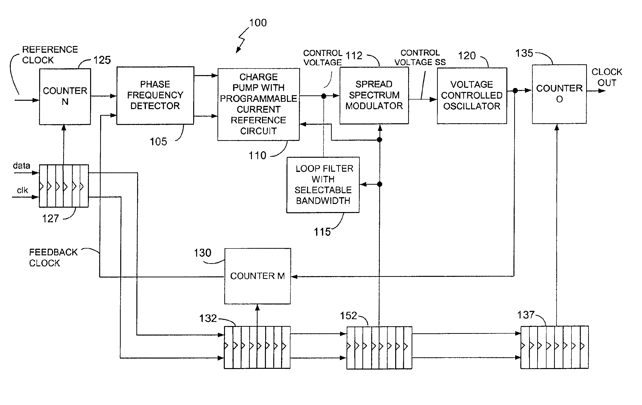
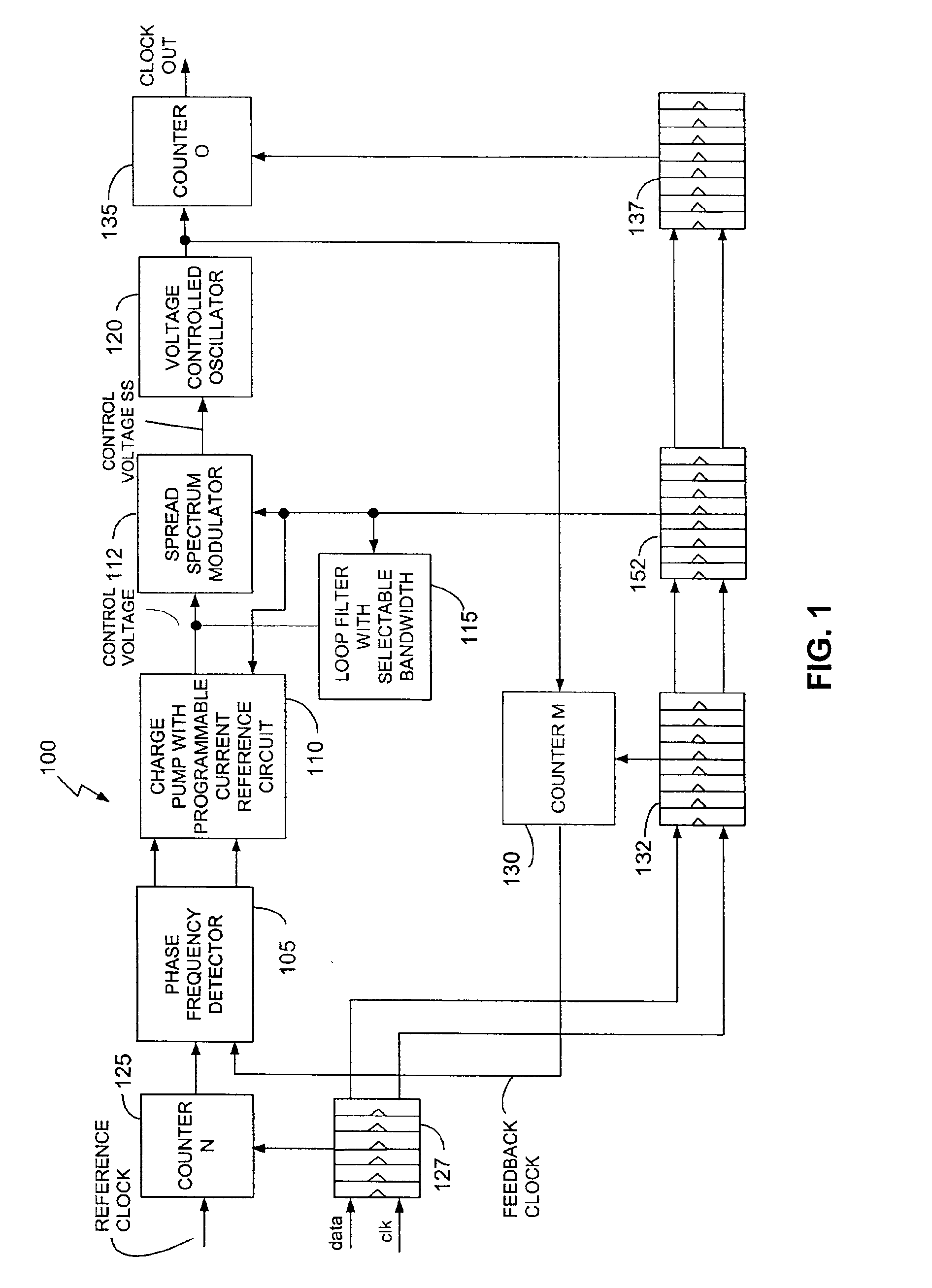
The present invention is a PLL circuit that includes a feedback loop and a programmable loop filter. The loop filter can provide different bandwidths and resistances to achieve desired performance. The feedback loop includes a detector and a signal generator. The technical effect of this invention is to provide a flexible and programmable PLL circuit that can improve the performance of electronic devices.

Problems solved by technology

This limits the usefulness of the PLL circuit.

Method used


Image

  • Programmable loop bandwidth in phase locked loop (PLL) circuit
  • Programmable loop bandwidth in phase locked loop (PLL) circuit
  • Programmable loop bandwidth in phase locked loop (PLL) circuit

Examples


second embodiment

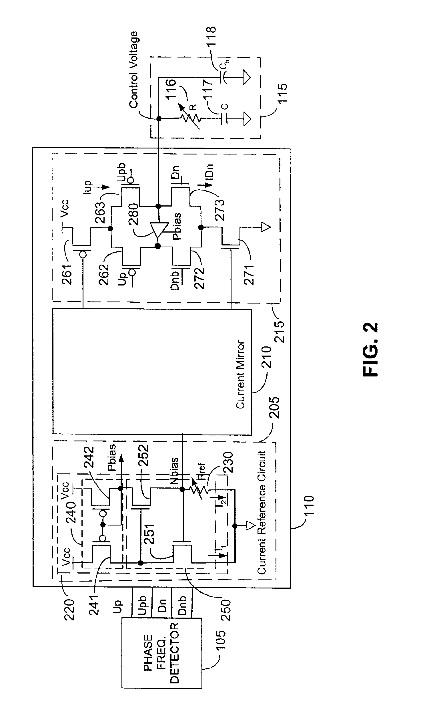
FIG. 4 is a detailed circuit diagram of the programmable bandwidth loop filter of the present invention. In FIG. 4, resistors R1 through RY are coupled in series, where Y is an integer and in this specific embodiment is equal to or greater than 3. More generally, Y is an integer equal to or greater than 1. As can be seen in FIG. 4, CMOS transistors 1 through Y are coupled across one or more of the resistors R1 through RY. In one embodiment, the CMOS transistors have a relatively small resistance. This allows to effectively short around the desired resistors in the series R1 through RY to obtain the desired overall resistance. In one embodiment, all of the resistors R1 through RY have the same resistance. In another embodiment, each of the resistors R1 and RY has a different resistance. By turning on one or more of the rip appropriate CMOS transistors and turning off the remaining CMOS transistors, a desired overall resistance may be obtained.

third embodiment

FIG. 5 is a detailed circuit diagram of the programmable bandwidth loop filter 115 of the present invention. In the embodiment shown in FIG. 5, each of CMOS transistors CMOS 1 to CMOSY provides a shorting path around one, rather than a plurality, of resistors R1 to RY. As can be seen in FIG. 5, transistors CMOS1 to CMOSY provide a shorting path around resistors R1 to RY, respectively.

In the embodiments shown in FIGS. 4 and 5, there are no CMOS transistors coupled in series with the resistors R1 to RY. In another embodiment, there may be a CMOS transistor coupled in series with resistors R1 to RY.

fourth embodiment

FIG. 6 is a detailed circuit diagram of the programmable bandwidth loop filter 115 of the present invention. In the embodiment shown in FIG. 6, there is a combination of both parallel and serial resistances. By turning on one or more of the appropriate CMOS transistors and turning off the remaining CMOS transistors, a desired overall resistance may be obtained. As can be seen in FIG. 6, turning on any one of CMOSY1 through CMOSYX would short all the resistors R11 through RYX. Thus, having only one of CMOSY1 through CMOSYX is sufficient for shorting all resistors R11 through RYX. In one embodiment, all of the resistors R11 through RYX have the same resistance. In another embodiment, each of the resistors R11 and RYX has a different resistance.


PUM


Abstract

A PLL circuit is described. The PLL circuit includes: a feedback loop and a loop filter coupled to the feedback loop, where the loop filter is programmable to provide one of a plurality of bandwidths. In one embodiment, the loop filter is programmable to provide one of a plurality of resistances, each resistance of the plurality of resistances corresponding to one of the plurality of bandwidths. In one embodiment, the feedback loop includes a detector and a signal generator coupled to the detector.

Description

BACKGROUND OF THE INVENTION1. Field of the InventionThis invention relates generally to electronic circuits and, in particular, to phase locked loop (PLL) circuits used in electronic circuits.2. Description of the Related ArtPLL circuits are used in many different context. In PLL circuits, an output frequency is locked into a reference frequency. The loop filter of a PLL circuit determines its operating bandwidth. In existing PLL circuits, the bandwidth of the loop filter is constant. Therefore, the operating bandwidth of the PLL circuit is also constant. This limits the usefulness of the PLL circuit.The present invention addresses this and other disadvantages of existing PLL circuits.SUMMARY OF THE INVENTIONThe present invention encompasses a PLL circuit. In one embodiment, the PLL circuit of the present invention includes: a feedback loop and a loop filter coupled to the feedback loop, where the loop filter is programmable to provide one of a plurality of bandwidths. In one embodi...

Claims


Application Information

Patent Timeline
Patent Type & Authority Patents(United States)
IPC IPC(8): H03L7/06H03L7/089H03L7/093H03L7/107H03L7/18
CPCH03L7/0896H03L7/0898H03L7/18H03L7/107H03L7/1075H03L7/093
Inventor STARR, GREGORY W.CHANG, WANLI
Owner ALTERA CORP
Learn More