Low-pass filter, feedback system, and semiconductor integrated circuit

Inactive Publication Date: 2006-07-18
PANASONIC CORP
View PDF13 Cites 67 Cited by
  • Summary
  • Abstract
  • Description
  • Claims
  • Application Information

AI Technical Summary

Benefits of technology

[0021]In this way, a filter having the same structure as that described above is used as a loop

Problems solved by technology

However, increasing the size of the capacitive element is causes an increase in the circuit size.
This is a serious problem especially in a semiconductor integrated circuit including a large number of PLLs, such as a microprocessor, or the like.
The countermeasure of externally providing a large capacitive element is substantially impossible.
In the above first and second examples, the objective of reducing the size of the capacitive element is achieved, but on the other hand, collateral problems emerge.
For example, in the first example, it is necessary to provide an adder c

Method used


Image

  • Low-pass filter, feedback system, and semiconductor integrated circuit
  • Low-pass filter, feedback system, and semiconductor integrated circuit
  • Low-pass filter, feedback system, and semiconductor integrated circuit

Examples


embodiment 1

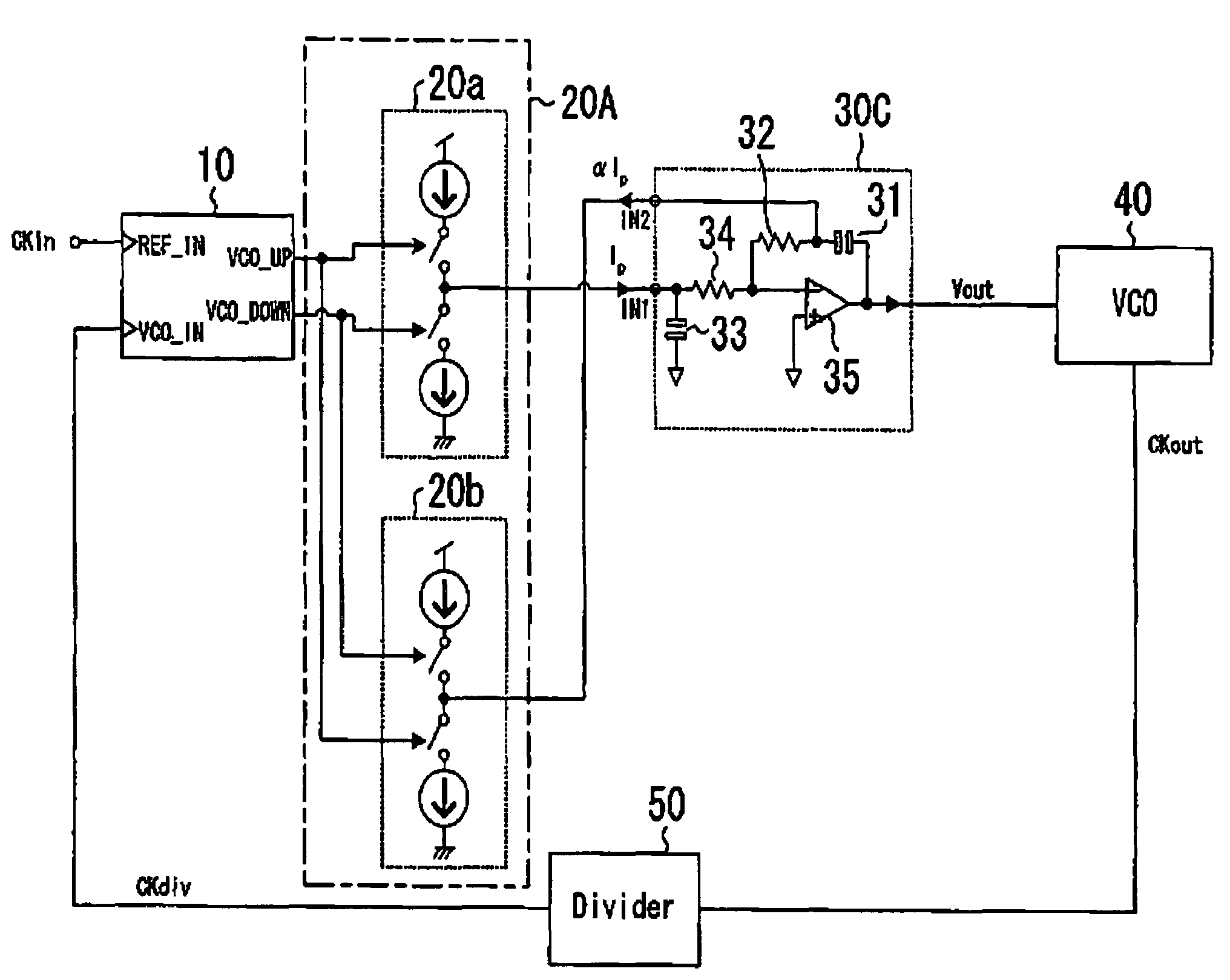
[0042]FIG. 1 shows the structure of a feedback system according to embodiment 1 of the present invention. The feedback system of embodiment 1 is a PLL including a phase comparator 10, a charge pump circuit 20A, a loop filter 30A, a voltage controlled oscillator (output clock generation means) 40, and a frequency divider 50. Among these components, the phase comparator 10, the voltage controlled oscillator 40, and the frequency divider 50 are as described above. Hereinafter, the charge pump circuit 20A and the loop filter 30A are described in detail.

[0043]The charge pump circuit 20A includes two general charge pump circuits (partial charge pump circuits) 20a and 20b. The charge pump circuit 20a outputs / receives electric current Ip according to signal UP and signal DN which are output from the phase comparator 10. The charge pump circuit 20b outputs / receives electric current αIp according to signal UP and signal DN. The direction of electric current αIp is opposite to that of electric...

embodiment 2

[0051]FIG. 3 shows the structure of a feedback system according to embodiment 2 of the present invention. The feedback system of embodiment 2 is a PLL including an active loop filter 30C, whereas the feedback system of embodiment 1 is a PLL including the passive loop filter 30A. The components of the PLL of embodiment 2 are as described in embodiment 1 except for the loop filter 30C. Hereinafter, the loop filter 30C is described in detail.

[0052]The loop filter 30C includes a capacitive element (first element block) 31, a resistive element (second element block) 32 connected in series to the capacitive element 31, a capacitive element (third element block) 33, a resistive element 34, and an operational amplifier 35. The output terminal of the operational amplifier 35 is connected to one end of the capacitive element 31. The inverted phase input terminal of the operational amplifier 35 is connected to a connection point of the resistive element 32 and the resistive element 34. The nor...

embodiment 3

[0061]FIG. 6 shows the structure of a feedback system according to embodiment 3 of the present invention. The feedback system of embodiment 3 is a delay locked loop circuit (hereinafter, referred to as “DLL”) including a phase comparator 10, a charge pump circuit 20C, a loop filter 30E, and a voltage controlled delay circuit (output clock generation means) 40. Hereinafter, the charge pump circuit 20C and the loop filter 30E are described in detail.

[0062]The charge pump circuit 20C includes current sources 21 and 23 for charge, which supply electric currents αIp and (1−α)Ip, respectively, and current sources 22 and 24 for discharge as does the above-described charge pump circuit 20B. When signal UP is supplied, control switches SW1 and SW3 are brought into conduction so that electric currents αIp and (1−α)Ip are released. On the other hand, when signal DN is supplied, control switches SW2 and SW4 are brought into conduction so that electric currents αIp and (1−α)Ip are sucked. That i...


PUM


Abstract

In a low-pass filter which is preferably used as a loop filter in a PLL or DLL, filter characteristics which are the same as those of a conventional low-pass filter are realized without causing collateral problems, such as an increase in the circuit area, the circuit complexity, or the resistance value, which may be caused due to size reduction of a capacitive element in the conventional low-pass filter. Thus, in a loop filter including a capacitive element and a resistive element which are connected in series, the first input terminal is provided at the side including the resistive element, and the second input terminal is provided at a connection point of the capacitive element and the resistive element. The first input terminal is supplied with the first electric current. On the other hand, the second electric current, which is a part of the first electric current supplied to the first input terminal, is extracted from the second input terminal, so that the electric current flowing into the capacitive element is smaller than the electric current flowing through the resistive element.

Description

BACKGROUND OF THE INVENTION[0001]The present invention relates to a low-pass filter and specifically to a technique of a low-pass filter suitable for use as a loop filter in a feedback system, such as a phase locked loop circuit, a delay locked loop, or the like.[0002]In currently-existing semiconductor integrated circuit systems, a feedback system, especially a phase locked loop circuit (hereinafter, referred to as “PLL”), is one of the indispensable components and is incorporated in almost all the LSI devices. The applications of the feedback system range over various technological fields, such as communication devices, microprocessors, IC cards, etc.[0003]FIG. 13 shows the structure of a general charge pump type PLL. General features of the PLL are described with reference to FIG. 13. A phase comparator 10 compares input clock CKin which is supplied to the PLL and feed back clock CKdiv and outputs up signal UP and down signal DN according to the phase difference between the compa...

Claims


Application Information

Patent Timeline
IPC IPC(8): H03L7/06H03L7/00H03L7/107H03H7/06H03H11/04H03H11/12H03L7/089H03L7/093H03L7/18H03L7/187
CPCH03H7/06H03H11/126H03L7/18H03L7/0895H03L7/093H03L7/0893A47K3/062F24H9/0052
Inventor DOSHO, SHIRO
Owner PANASONIC CORP
Why Eureka
Try Eureka