
Socket for electrical parts

a technology for electrical parts and sockets, applied in the direction of coupling contact members, coupling device connections, electrical apparatus construction details, etc., can solve the problems of reducing the opening degree of the contact portion of the contact pin, and reducing the lowering amount. , to achieve the effect of removing defects or drawbacks

Inactive Publication Date: 2005-02-22
ENPLAS CORP
View PDF3 Cites 2 Cited by
  • Summary
  • Abstract
  • Description
  • Claims
  • Application Information

AI Technical Summary

Benefits of technology

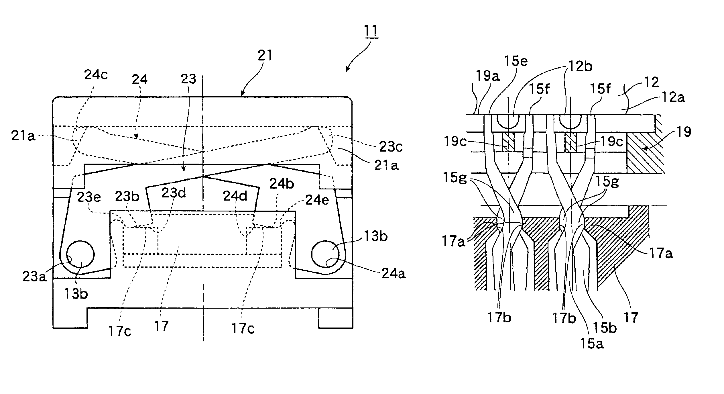
The present invention provides a socket for an electrical part that prevents wear and damage to the contact pins and ensures a suitable moving amount of the movable member. This is achieved by eliminating defects in the prior art by providing a socket body with a number of contact pins, a movable member, and a lever member mounted to the socket body to be rotatable. The lever member has a pressing portion that acts to press a portion of the movable member in response to the rotation of the lever member. The pressed portion of the movable member and the pressing portion of the lever member achieve surface-to-surface contact to each other, reducing the applied force and ensuring a maximum lowering amount of the movable member. This design prevents the contact pins from being worn or broken and ensures a suitable moving amount of the movable member even after repeated operation.

Problems solved by technology

If an IC socket having such structure is used repeatedly, the pressed portion of the movable member made of synthetic resin will be worn or broken because the movable member is made of synthetic resin where as the lever member is made of metal material.
The wearing or breaking of the pressed portion of the movable member will result in the reduction of the lowering amount of the movable member and, hence, an opening degree of the contact portion of the contact pin cannot be ensured to an amount capable of receiving the solder ball in the contacting / separating manner.

Method used


Image

  • Socket for electrical parts
  • Socket for electrical parts
  • Socket for electrical parts

Examples


Embodiment Construction

[0044]A preferred embodiment of the present invention will be described hereunder with referenced to FIGS. 1 to 13.

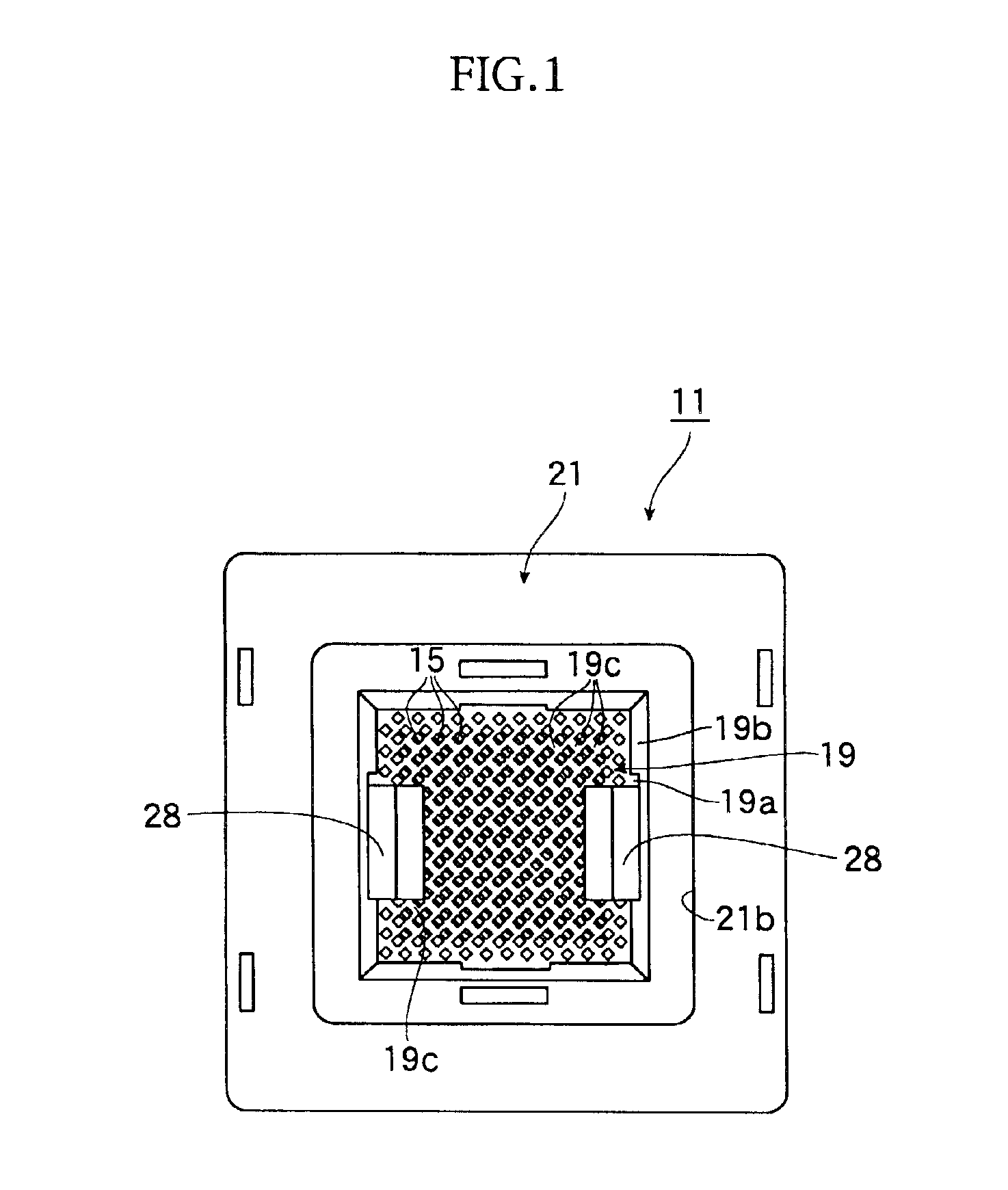
[0045]In the drawings, reference numeral 11 denotes an IC socket as “socket for an electrical part”. This IC socket 11 is a socket for achieving an electrical connection between a solder ball 12b as “terminal” of an IC package 12 as “electrical part” and a printed circuit board, not shown, of a tester for carrying out a performance test of the IC package 12.

[0046]The IC package 12 is so-called a BGA (Ball Grid Array) type, as shown in FIGS. 10A and 10B, in which a number of spherical solder balls 12b are arranged on a lower surface of a square package body 12 of the IC package 12 in form of matrix including vertical and horizontal rows.

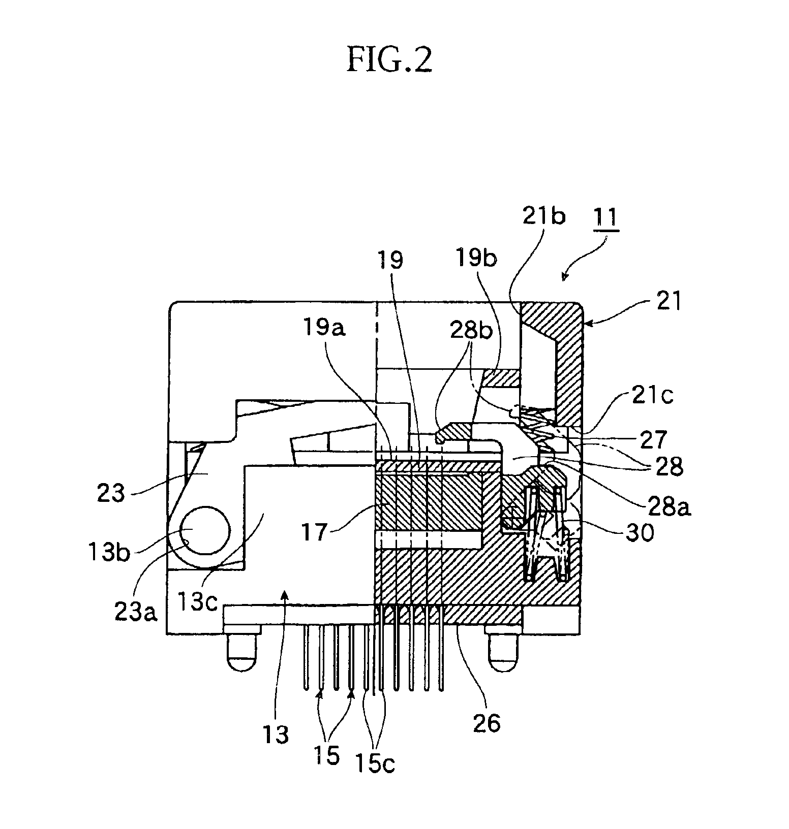
[0047]On the other hand, the IC socket 11 comprises, as shown in FIG. 2, a socket body 13 which is made of synthetic resin, mounted on the printed circuit board to which contact pins 15 are arranged so as to be contacted to or separated f...


PUM


Abstract

A socket for an electrical part has a socket body to which an IC package as an electrical part is accommodated, the socket body being provided with a number of contact pins which are contacted to or separated from solder balls as terminals of the electrical part, a movable member arranged to be movable with respect to the socket body, and lever members mounted to both sides of the socket body to be rotatable. In this structure, when the lever members are rotated, the movable member is moved to displace the contact pins so as to be contacted to or separated from the solder balls of the electrical part, respectively. In such structure, each of the lever members are formed with pressing portion which acts to press a portion of the movable member in accordance with the rotation of the lever members and when the movable member is moved so as to approach a lowermost position thereof by the rotation of the lever member, the pressing portion and the pressed portion achieves surface-to-surface contact to each other.

Description

BACKGROUND OF THE INVENTION[0002]1. Field of The Invention[0003]The present invention relates to a socket for an electrical part for detachably holding an electrical part such as semiconductor device (called “IC package” hereinlater).[0004]2. Related Art of the Invention[0005]In a known art, there has been provided an IC socket, as “socket for an electrical part” of a kind mentioned above, for accommodating an IC package as “electrical part”.[0006]In such IC package, a number of solder balls as “terminals” are provided so as to project from a lower surface of the IC package and these solder balls are arranged in lattice having vertical and horizontal rows.[0007]On the other hand, the IC socket has a socket body into which the IC package is accommodated and to which a number of contact pins contacting the terminals of the IC package are arranged. The socket body is also provided with a movable member, which is urged upward to be vertically movable by means of coil spring, for elastic...

Claims


Application Information

Patent Timeline
Patent Type & Authority Patents(United States)
IPC IPC(8): H01R13/24H01R13/629H01R13/22H01R24/00H01R33/76H01R107/00
CPCH05K7/1084H01R13/629
Inventor HAYAKAWA, KENJI
Owner ENPLAS CORP
Learn More