Semiconductor device capable of accurately producing internal multi-phase clock signal
- Summary
- Abstract
- Description
- Claims
- Application Information
AI Technical Summary
Benefits of technology
Problems solved by technology
Method used
Image
Examples
first embodiment
[First Embodiment]
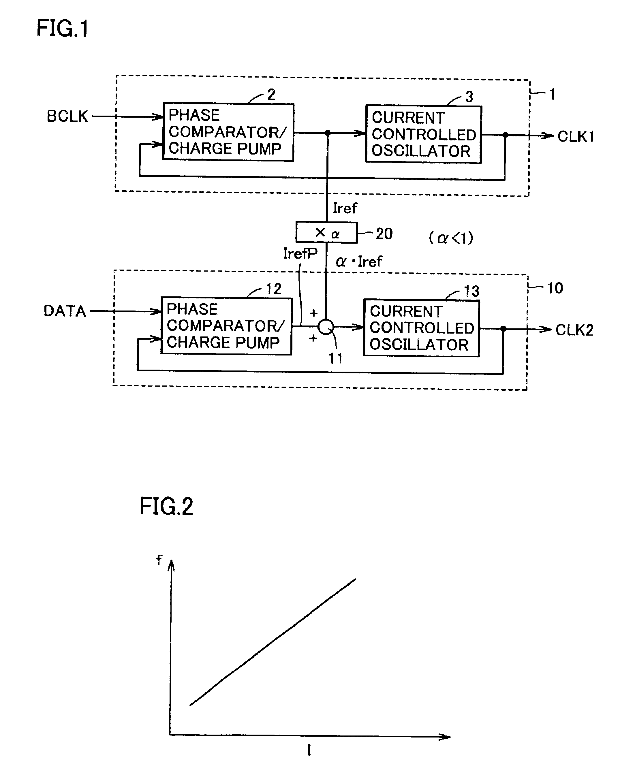
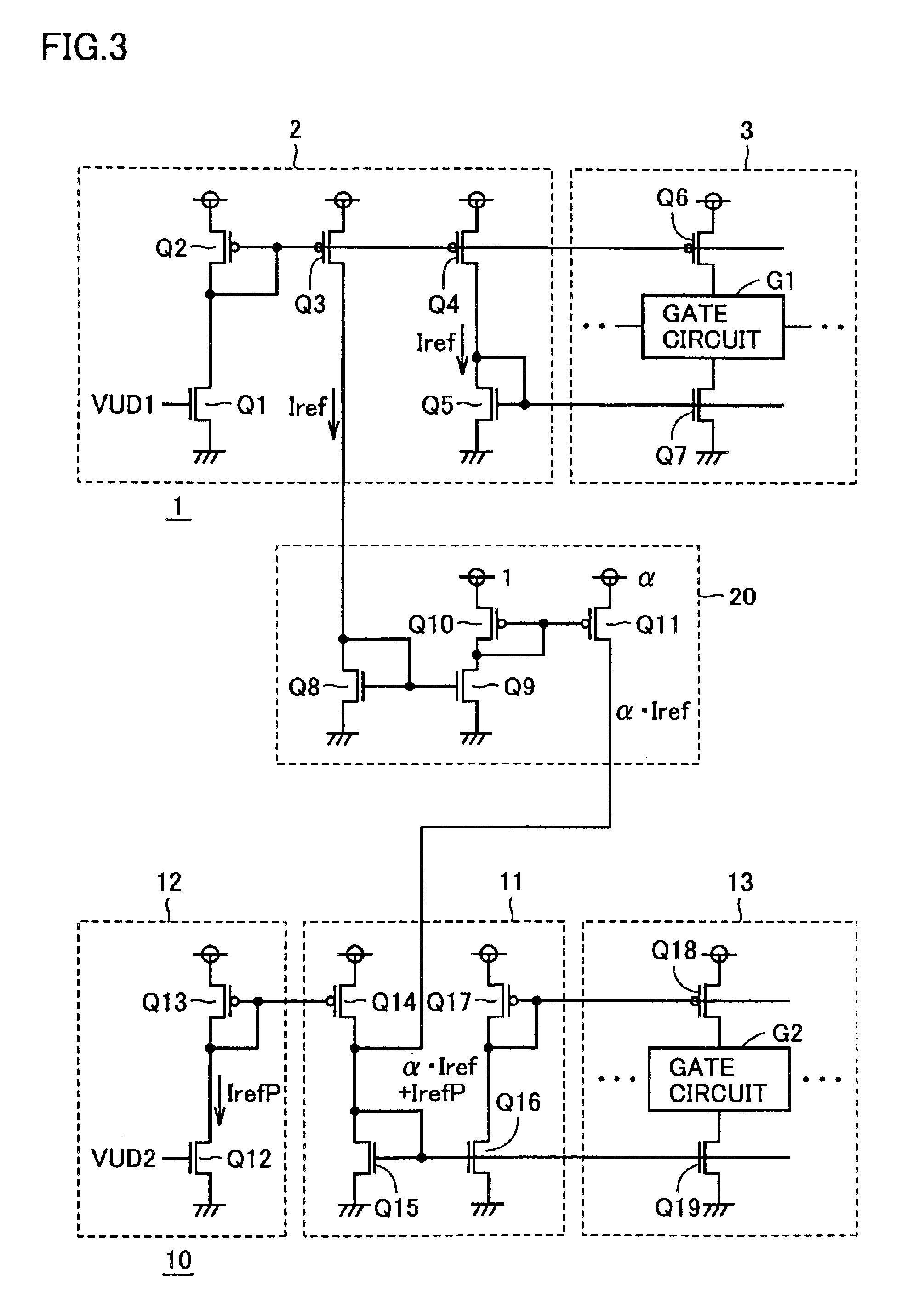
FIG. 1 is a diagram schematically showing a configuration of a semiconductor device in accordance with a first embodiment of the present invention. In FIG. 1, this semiconductor device includes a first internal clock generating circuit 1 for generating a first internal clock signal CLK1 synchronized with a basic clock signal BCLK, and a second internal clock generating circuit 10 for generating a second internal clock signal CLK2 synchronized with external data DATA that is a synchronization object signal.
Basic clock signal BCLK is a basic clock signal in this semiconductor device, and external data DATA has its phase slightly shifted with respect to this basic clock signal BCLK.
First internal clock signal CLK1 is used for data output and internal processing in this semiconductor device. Second internal clock signal CLK2 is used in a circuit for processing external data DATA. External data DATA is, for example, external data (or a packet) in a communication system,...
second embodiment
[Second Embodiment]
FIG. 4 is a diagram schematically showing a configuration of a semiconductor device in accordance with a second embodiment of the present invention. In a configuration shown in FIG. 4, first internal clock generating circuit 1 has the same configuration as shown in FIG. 1, and includes phase difference detecting circuit 2 and current controlled oscillator 3 performing an oscillation operation in accordance with reference current Iref outputted by phase difference detecting circuit 2.
Reference current Iref generated by first internal clock generating circuit 1 is applied to second internal clock generating circuit 10, not through a multiplier. In other words, multiplier 20 shown in FIG. 1 is not provided between internal clock generating circuits 1 and 10.
Second internal clock generating circuit 10 is different from second internal clock generating circuit 10 shown in FIG. 1 in its configuration in the following point. An addition circuit 21 for combining reference...
third embodiment
[Third Embodiment]
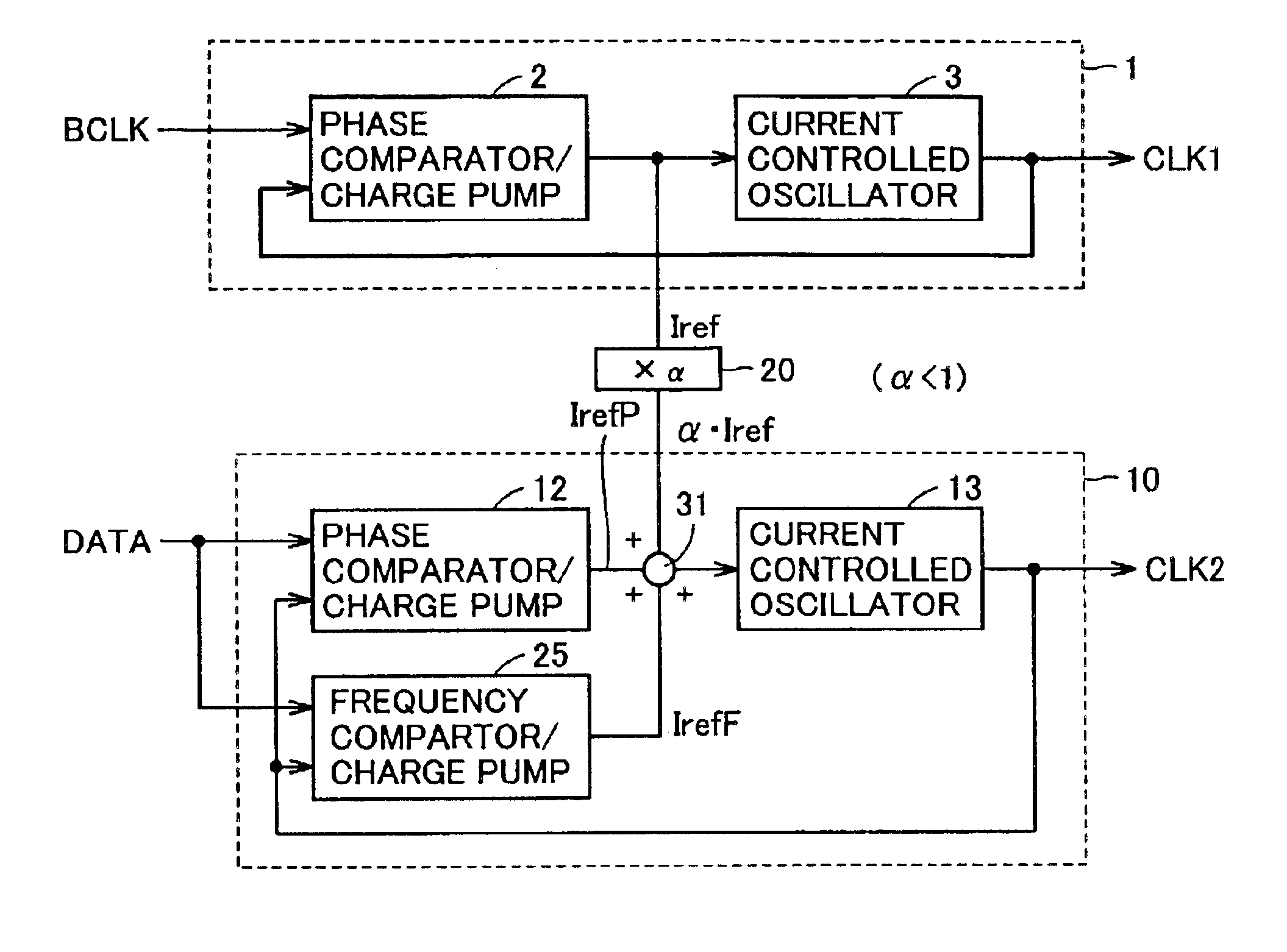
FIG. 6 is a diagram schematically showing a configuration of a semiconductor device in accordance with a third embodiment of the present invention. In the semiconductor device shown in FIG. 6, the configuration of second internal clock generating circuit 10 differs from that of the internal clock generating circuit shown in FIG. 1. More specifically, in second internal clock generating circuit 10, there are provided a frequency difference detecting circuit 25 for comparing external data DATA with second internal clock signal CLK2 in frequency and generating a frequency error current IrefF in accordance with a result of comparison, and an addition circuit 31 for performing an addition of standard reference current α·Iref outputted by multiplier 20 and the outputs IrefP and IrefF of phase difference detecting circuit 12 and frequency difference detecting circuit 25.
Frequency difference detecting circuit 25 includes a frequency comparator for comparing in frequency ex...
PUM
 Abstract
Description
Claims
Application Information


