

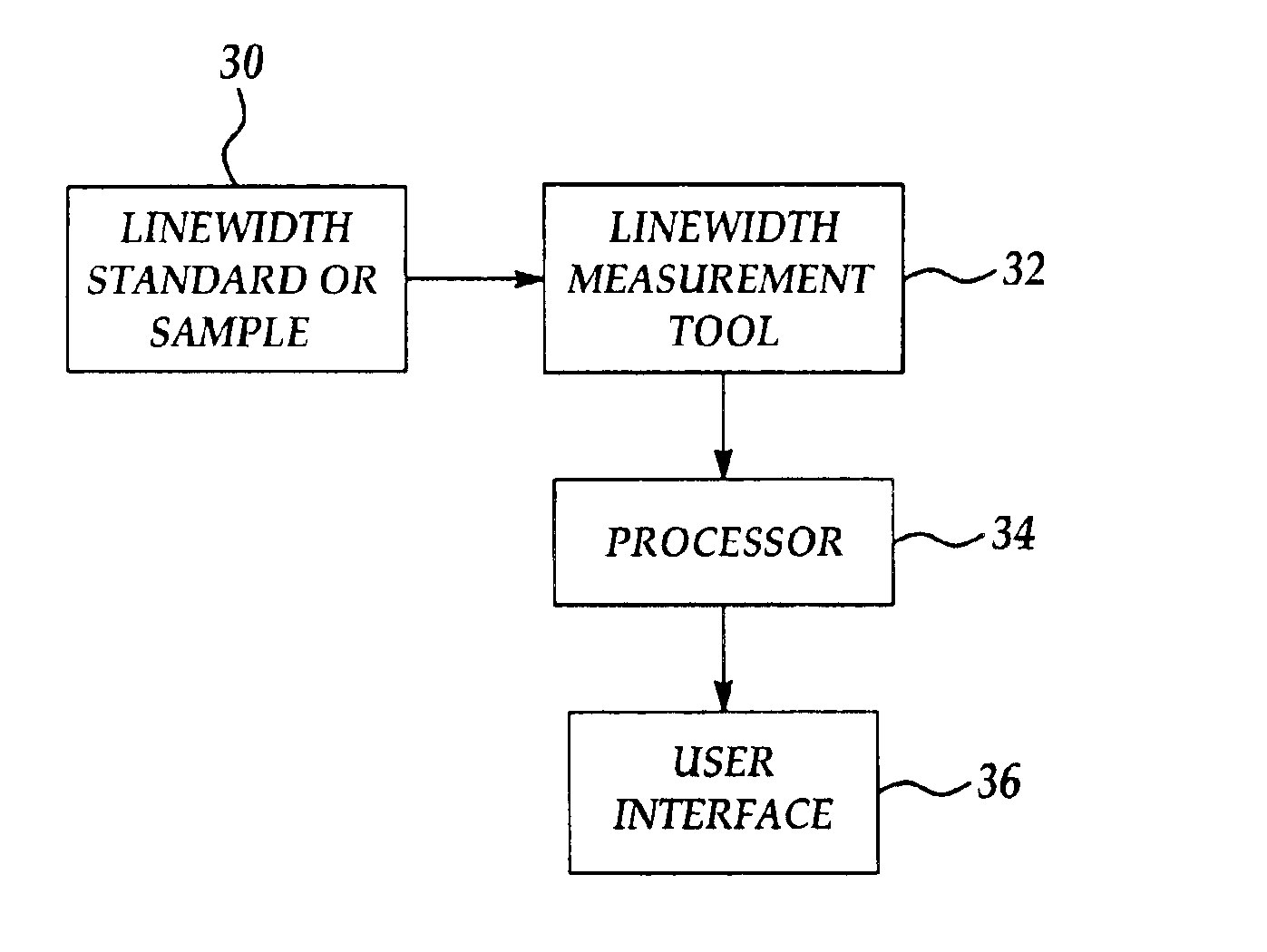
Linewidth measurement tool calibration method employing linewidth standard
- Summary
- Abstract
- Description
- Claims
- Application Information
AI Technical Summary
Benefits of technology
Problems solved by technology
Method used
Image

Examples
Embodiment Construction
The present invention provides a method for monitoring a linewidth of a patterned layer when fabricating a microelectronic product, wherein the method provides for accurate monitoring of the linewidth of the patterned layer.
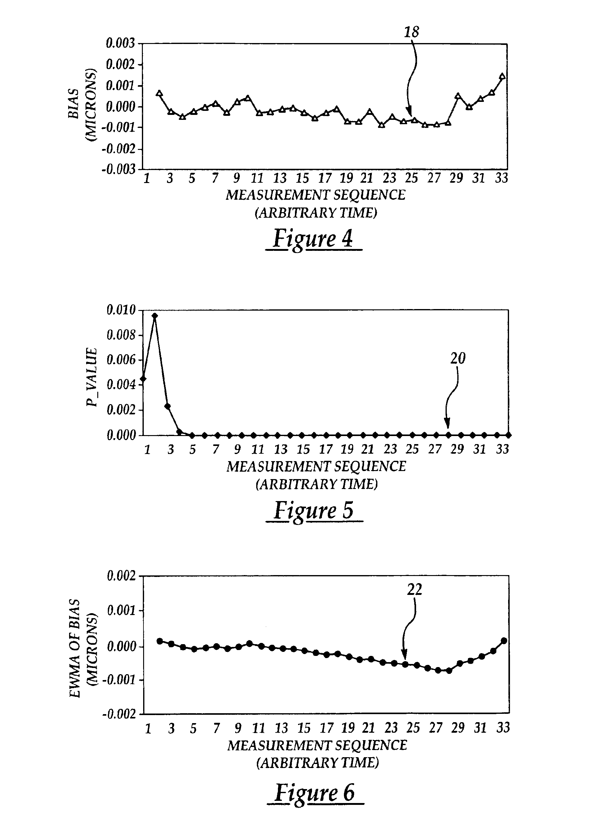
The invention realizes the foregoing object by correcting each of a series of periodic actual measurements of at least one single measurement location of a topographic feature within a linewidth standard with an exponentially weighted moving average of a series of deviations of the series of periodic actual measurements from a corresponding series of regressed data points derived from mathematical regression of the series of periodic actual measurements.
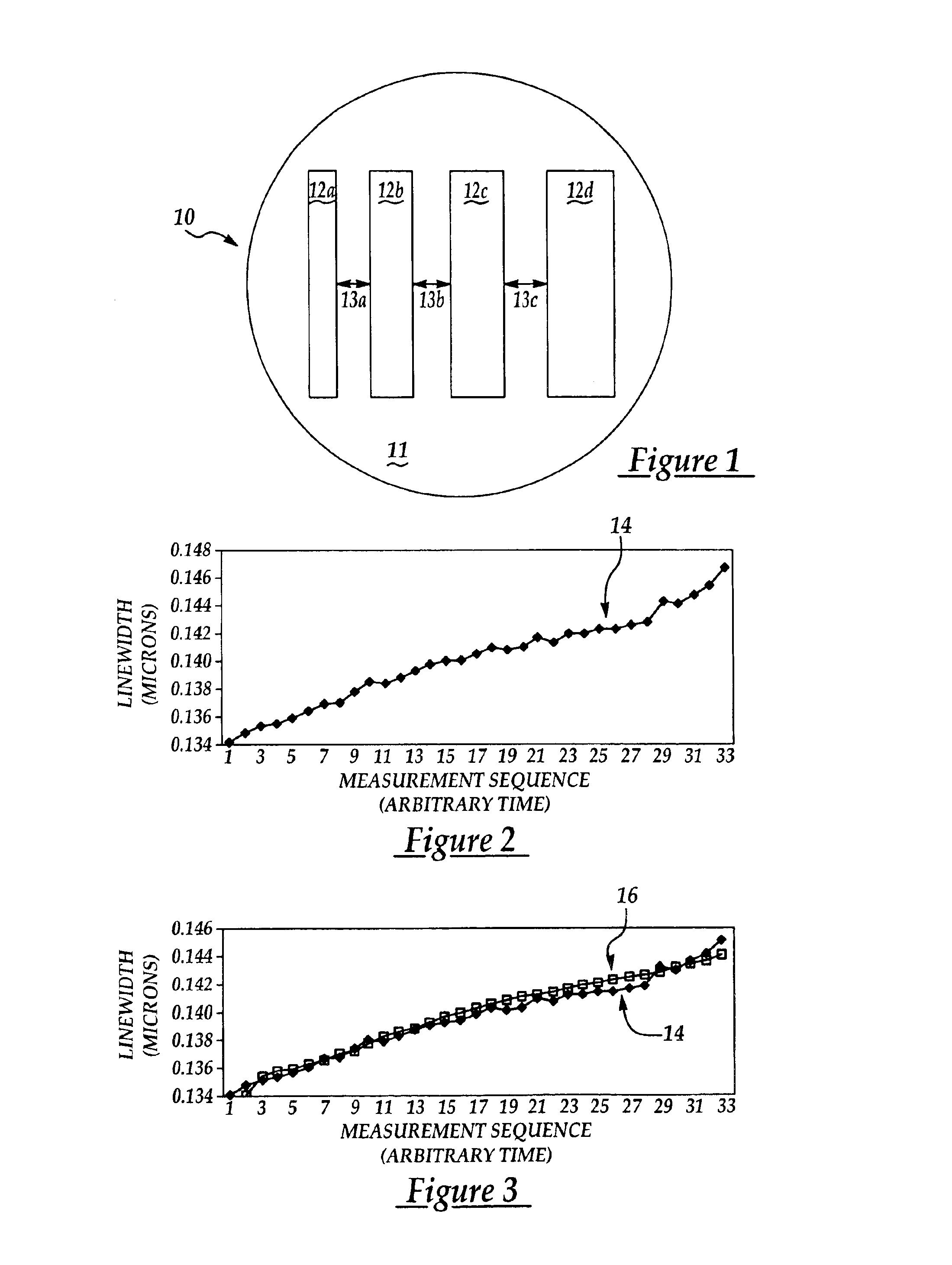
FIG. 1 illustrates a schematic plan view diagram of a linewidth standard which may be employed within the context of the invention.
Within FIG. 1, a linewidth standard 10 comprises a substrate 11 having formed thereupon a series of lines 12a, 12b, 12c and 12d separated by a series of gaps 13a, 13b and 13c.
Within t...
PUM
 Abstract
Description
Claims
Application Information