Method of manufacturing a probe card

a technology of probe cards and manufacturing methods, applied in the direction of individual semiconductor device testing, semiconductor/solid-state device testing/measurement, instruments, etc., can solve the problem manufacturing a probe card assembly, and achieve the effect of shortening the process of designing

Inactive Publication Date: 2005-03-08
FORMFACTOR INC
View PDF45 Cites 98 Cited by
  • Summary
  • Abstract
  • Description
  • Claims
  • Application Information

AI Technical Summary

Benefits of technology

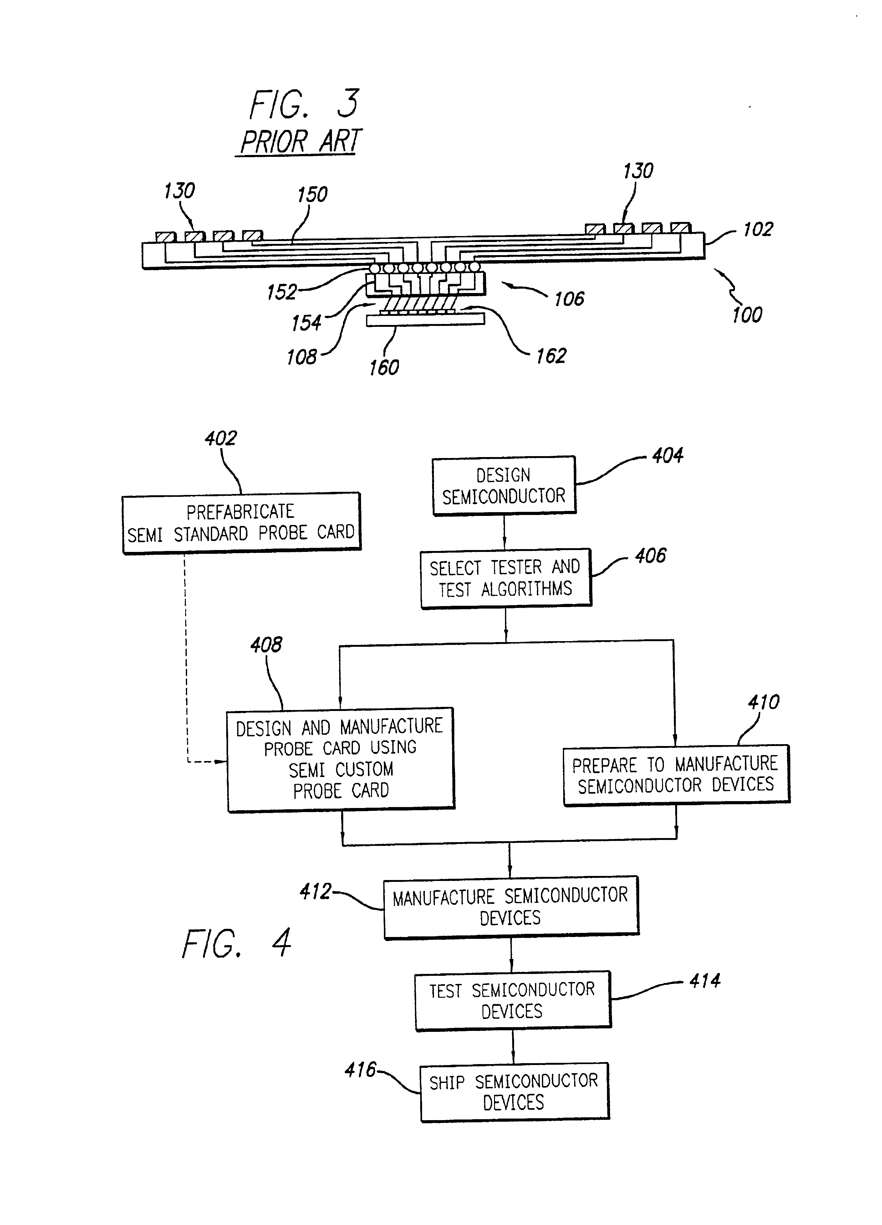
The invention relates generally to methods of making probe card assemblies, which are used to test semiconductor devices. One or more elements of the probe card assembly is prefabricated to one or more predefined designs. Thereafter, design data regarding a newly designed semiconductor device is received along with data describing the tester and testing algorithms to be used to test the semiconductor device. Using the received data, one or more of the prefabricated elements is selected. Again using the received data, one or more of the selected prefabricated elements is customized. The probe card assembly is then built using the selected and customized elements. The use of prefabricated elements shortens the process of designing and manufacturing a probe card assembly.

Problems solved by technology

The use of prefabricated elements shortens the process of designing and manufacturing a probe card assembly.

Method used


Image

  • Method of manufacturing a probe card
  • Method of manufacturing a probe card
  • Method of manufacturing a probe card

Examples


example 1

TABLE IIDistance fromPad size“A”“B”“C”“D”“E”center (in.):(mils):(mils):(mils):(mils):(mils):(mils):  0-0.257.421269.0212628.8212614.4206335.421269.021260.26-0.5 9.9212611.5212631.3212615.6606337.9212611.521260.51-0.7512.4212614.0212633.8212616.9106340.4212614.021260.76-1.0 14.9212616.5212636.3212618.1606342.9212616.52126>1.017.4212619.02112638.8212619.4106345.4212619.021126

example 2

TABLE IIIDistance fromPad size“A”“B”“C”“D”“E”center (in.):(mils):(mils):(mils):(mils):(mils):(mils):  0-0.257.4212610.2712630.0712615.0356336.6712610.271260.26-0.5 9.9212610.2712630.0712615.0356336.6712610.271260.51-0.7512.4212615.2712635.0712617.5356341.6712615.271260.76-1.0 14.9212615.2712635.0712617.5356341.6712615.27126>1.017.4212615.2712635.0712617.5356341.6712615.27126

example 3

TABLE IVDistance fromPad size“A”“B”“C”“D”“E”center (in.):(mils):(mils):(mils):(mils):(mils):(mils):  0-0.257.4212612.7712632.5712616.2856339.1712612.771260.26-0.5 9.9212612.7712632.5712616.2856339.1712612.771260.51-0.7512.4212612.7712632.5712616.2856339.1712612.771260.76-1.0 14.9212617.7712637.5712618.7856344.1712617.77126>1.017.4212617.7712637.5712618.7856344.1712617.77126

By way of explanation, and referring to Example 1 above (Table II), those signal pads in the second horizontal group of pads 3006 whose center point is located between 0 and 0.25 inches from center point 3019 would be generally square with sides of about 7.42126 mils in length. The vertical spacing (spacing “A”) between the pads in such a column of signal pads (e.g., columns 3202, 3204, 3206, 3208, 3210) would be 9.02126 mils, and the horizontal spacing (spacing “D”) between the column and the adjacent column moving away from center line 3018 would be 35.42126 mils.

Still referring to Example 1 above (Table II) but...


PUM

PropertyMeasurementUnit
lengthaaaaaaaaaa
lengthaaaaaaaaaa
lengthaaaaaaaaaa

Abstract

A method of designing and manufacturing a probe card assembly includes prefabricating one or more elements of the probe card assembly to one or more predefined designs. Thereafter, design data regarding a newly designed semiconductor device is received along with data describing the tester and testing algorithms to be used to test the semiconductor device. Using the received data, one or more of the prefabricated elements is selected. Again using the received data, one or more of the selected prefabricated elements is customized. The probe card assembly is then built using the selected and customized elements.

Description

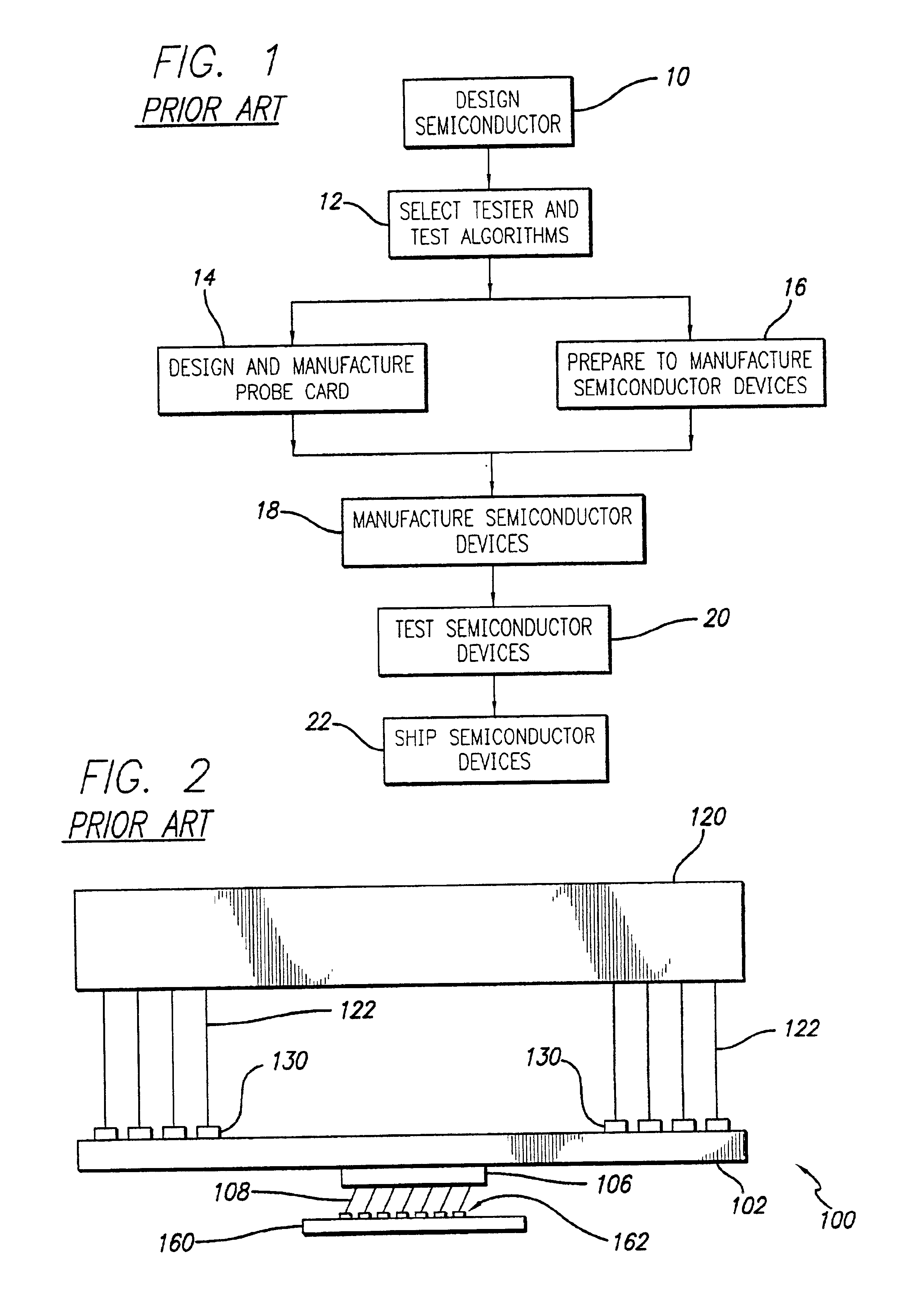
BACKGROUND OF THE INVENTION1. Field of the InventionThe present invention relates generally to an improved method of designing and manufacturing a probe card assembly and more specifically to use of prefabricated elements to speed design and manufacture of the probe card assembly.2. General Background and Related ArtFIG. 1 illustrates a simplified overview of a typical flow of common activities involved in designing and manufacturing a semiconductor device, such as a microelectronic “chip.” Initially, the semiconductor device is designed 10, and a tester and testing algorithms are selected and / or designed 12 for testing the semiconductor device. Using data regarding the semiconductor device design, the tester, and / or the test algorithms, a probe card for testing the semiconductor device is then custom designed 14. Usually concurrently, preparations are made to begin manufacturing the semiconductor device in commercial quantities 16. Once the probe card is designed and manufactured a...

Claims


Application Information

Patent Timeline
Patent Type & Authority Patents(United States)
IPC IPC(8): G01R1/073G01R31/28G01R31/26H01L21/66
CPCG01R1/07314G01R1/07378G01R3/00G01R31/2886G01R31/2889G01R1/07342Y10T29/49147Y10T29/49117Y10T29/49149Y10T29/49004Y10T29/49124Y10T29/49453Y10T29/4913Y10T29/49002Y10T29/49126G01R1/07357G01R1/073
Inventor GRUBE, GARY W.KHANDROS, IGOR Y.ELDRIDGE, BENJAMIN N.MATHIEU, GAETAN L.LOTFIZADEH, POYATSENG, CHIH-CHIANG
Owner FORMFACTOR INC
Why Eureka
Try Eureka