Voltage mode differential driver and method

a voltage mode and driver technology, applied in the direction of amplifiers, transmission lines, transmission lines, etc., can solve the problems of i/o design massive parallelism, i/o structures occupying more and more space on ics, and reducing the i/o bandwidth, so as to achieve low impedance and low impedance

Inactive Publication Date: 2005-03-15
AVAGO TECH INT SALES PTE LTD
View PDF14 Cites 73 Cited by
  • Summary
  • Abstract
  • Description
  • Claims
  • Application Information

AI Technical Summary

Benefits of technology

According to an embodiment of the present invention, a differential driver is provided. The differential driver includes a switching module and first and second voltage controlled voltage sources. The switching module has a plurality of switches each controlled by an input signal, a first voltage input and a second voltage input, and a signal output. The first voltage controlled voltage source is connected to the first voltage input. The first voltage controlled voltage source has a low impedance. The second voltage controlled voltage source is connected to the second voltage input. The second voltage controlled voltage source also has a low impedance. The switching circuit outputs an output signal having an output voltage and current controlled by the first and second voltage controlled voltage sources. The output signal is based upon the input signal.
According to another embodiment of the present invention, a method of driving a signal is provided. The method includes a step of providing a switching module having a first and second voltage input, a signal input, and a signal output. The signal input is connected to a plurality of switches in order to control an operation of the switches. The signal output is connected to the first and second voltage inputs via the plurality of

Problems solved by technology

In conventional I/O designs, high-speed data rates are accomplished with parallel I/O structures, each I/O device typically having a limited bandwidth.
Over the years, bandwidth has increased substantially leading to massive parallelism in I/O designs in ICs.
As a result, these parallel I/O structures occupy more and more space on ICs.
This complicates the design of the circuits because there is less available space on the chip.
Thus, most existing I/O drivers are not power efficient.
In the case where power is not restricted, such as in a desk top PC, power consumption is also important in IC.
For example, if a CPU consumes more power, it will require an expensive package for the IC an

Method used


Image

  • Voltage mode differential driver and method
  • Voltage mode differential driver and method
  • Voltage mode differential driver and method

Examples


Embodiment Construction

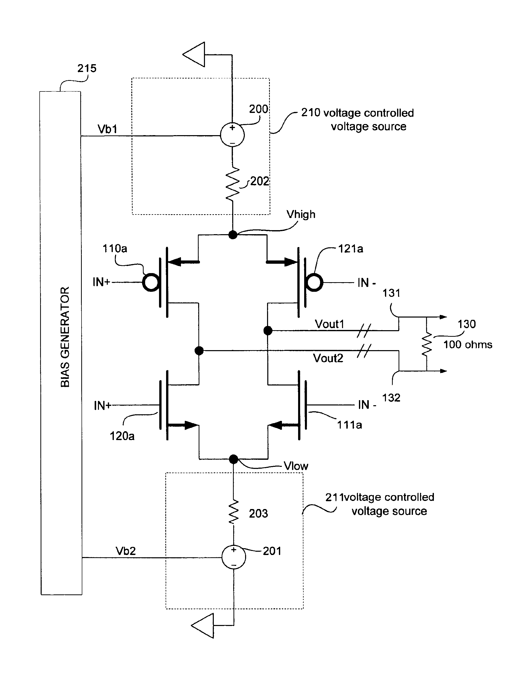
FIG. 3 is an illustration of a voltage mode differential driver according to an embodiment of the present invention. The differential driver includes two Voltage Controlled Voltage Sources (VCVS) 210 and 211, which provide DC voltages to the nodes Vhigh and Vlow, respectively. The output impedance for voltage controlled voltage source 210 is modeled by a resistor 202 and is configured to be a low impedance in the range of a few hundred ohms, preferable around 30 ohms for a differential load of 100 ohms. Similarly, the output impedance for the voltage controlled voltage source 211 is modeled by resistor 203 and is similarly configured to be a low impedance. VCVS 210 and 211 are biased by bias voltages Vb1 and Vb2, respectively output by a bias generator 215.

The differential driver also includes a switching circuit having a plurality of switches for switching an output voltage (signal) based on an input signal. The switching circuit may include a pair of voltage inputs, at nodes Vhigh...


PUM


Abstract

A differential driver includes a switching module and first and second voltage controlled voltage sources. The switching module has a plurality of switches each controlled by an input signal, a first voltage input and a second voltage input, and a signal output. The first voltage controlled voltage source is connected to the first voltage input. The first voltage controlled voltage source has a low impedance. The second voltage controlled voltage source is connected to the second voltage input. The second voltage controlled voltage source also has a low impedance. The switching circuit outputs an output signal having an output voltage and current controlled by the first and second voltage controlled voltage sources. The output signal is based upon the input signal.

Description

BACKGROUND OF THE INVENTION1. Field of the InventionThe invention relates to input / output (I / O) interface circuitry for high speed data communications applications. More specifically the invention relates to low voltage differential signaling (LVDS) drivers, for use in the fields of communications, video and other integrated circuits that demand very high data transfer rates.2. Description of the Related ArtDifferential drivers are well known. Differential drivers are used in many input / output (I / O) applications such as in communications, video and integrated circuits that may demand high data transfer rate. Differential drivers are used in integrated circuits (IC) for on-chip communications between circuits, chip-to-board, off-chip communications, etc.Low-voltage differential signaling (LVDS) technology was developed in order to provide a low-power and low-voltage alternative to other high-speed I / O interfaces specifically for point-to-point transmissions, such as those used in a n...

Claims


Application Information

Patent Timeline
IPC IPC(8): H03K5/24H03K5/22H03F3/45H04L25/02
CPCH03F3/45237H04L25/028H03K5/2481H04L25/0272H03F2203/45466H03F2203/45496H03F2203/45694H03F2203/45508
Inventor LI, NINGSHIEH, JIANN-CHYI SAM
Owner AVAGO TECH INT SALES PTE LTD
Why Eureka
Try Eureka