Device for detecting the angle of incidence of radiation on a radiation incidence surface

a radiation incidence surface and radiation detection technology, applied in the direction of optical radiation measurement, radiation control devices, instruments for comonautical navigation, etc., can solve the problems of optical disturbance and incidence angl

Active Publication Date: 2005-04-05
ELMOS SEMICON SE
View PDF5 Cites 46 Cited by
  • Summary
  • Abstract
  • Description
  • Claims
  • Application Information

AI Technical Summary

Benefits of technology

The shielding of the shading mask, e.g. for protection from damage, can be performed e.g. by an optically “dense” passivation layer, as basically known in semiconductor technology. Onto this layer, a plastic material will be applied, as known e.g. from optical elements or components in photo electronics. The sunlight incident onto the plastic layer from the optically thinner m

Problems solved by technology

This is perceived of as optically disturbing.
In the known devices, a certain disadvantage is seen in the fact that

Method used


Image

  • Device for detecting the angle of incidence of radiation on a radiation incidence surface
  • Device for detecting the angle of incidence of radiation on a radiation incidence surface
  • Device for detecting the angle of incidence of radiation on a radiation incidence surface

Examples


Embodiment Construction

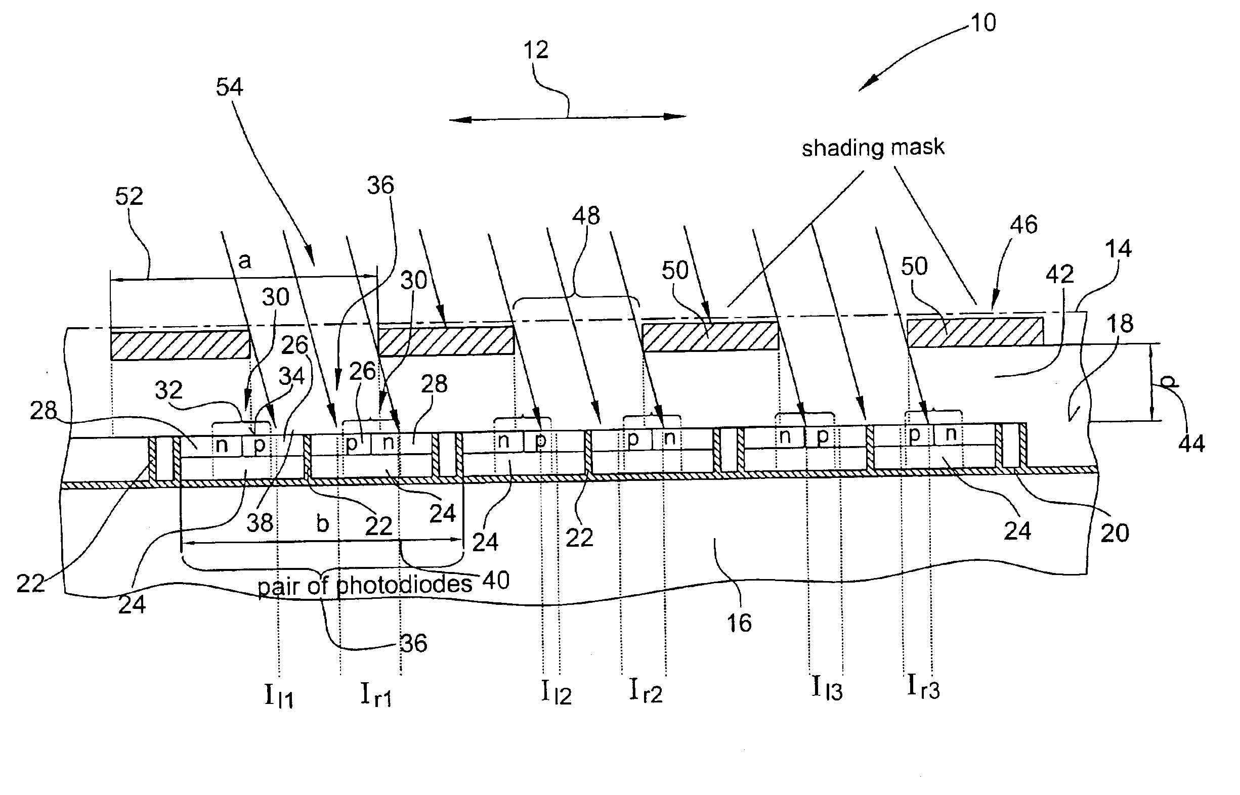
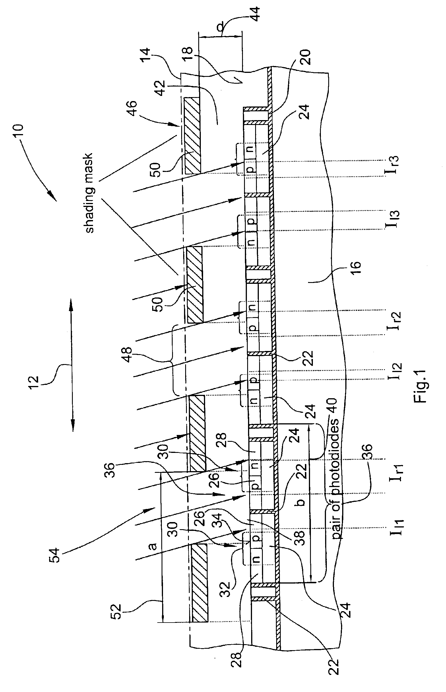
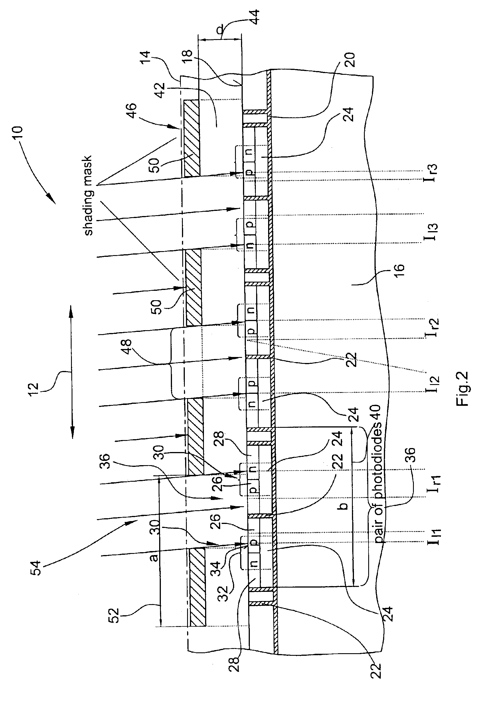
FIGS. 1 to 3 illustrate the basic configuration of a device 10 for detecting the angle of incidence of that component of a radiation which impinges onto a radiation incidence surface 14 along the axis marked by the twin arrow 12. Device 10 comprises a semiconductor substrate 16 which in the present case is provided as a SOI substrate and includes a horizontal insulating layer 20 extending below the surface 18 of substrate 16. Formed in the surface 18 of substrate 16 are vertical insulating trenches 22 so that the surface 18 of substrate 16 is provided with individual areas 24 dielectrically insulated from each other. In each of these areas 24, a p-doped region 26 and an n-doped region 28 of a photodiode 30 are inserted. Each photodiode 30 comprises a space-charge zone 32 having a space-charge zone face 34 arranged in the surface 18 of substrate 16.

Respectively two adjacent photodiodes 30 are connected to each other to form a pair 36 of photodiodes (not shown). The p- and n-regions 2...


PUM


Abstract

A device for detecting the angle of incidence of radiation on a radiation incidence surface (14) comprises at last two first pairs (36) of photodiodes comprising first photodiodes (30) arranged along a first axis (12) and connected in series in a pair-wise manner. Each of the first photodiodes (30) comprises a space-charge zone (32) having a space-charge zone face (34) oriented towards the radiation incidence face (14). Further, the device is provided with a a shading mask (46) arranged at a distance (44) above the space-charge zone faces (34) of the first photodiodes (30) and comprising radiation-transmitting areas (48). Each radiation-transmitting area (48) is assigned to the space-charge zone faces (34) of the two first photodiodes (30) of a first pair (36) of photodiodes. When viewed in the direction of the normal of the radiation incidence face (14), the degree of overlapping between a radiation-transmitting area (48) and its assigned space-charge zone faces (34) in the direction of the first axis (12) is different for at least two of the first pairs (36) of photodiodes. The device also comprises an evaluation unit (56) for monitoring the photocurrent and/or the photovoltage of each first photodiode (30) of each first pair (36) of photodiodes and for detecting, on the basis of a comparison of the photocurrents and/or the photovoltages, the angle of incidence under which the component of the radiation which in the projection is directed parallel to the first axis (12) impinges on the radiation incidence face (14).

Description

BACKGROUND OF THE INVENTION1. Field of the InventionThe present invention relates to a device for detecting the angle of incidence of radiation on a radiation incidence surface.2. Description of Related ArtIn a large number of applications, it is convenient to be able to measure the angle of incidence of radiation on a radiation incidence surface by use of measurement technology. Thus, for instance, in the field of air conditioning systems for automobiles, solar sensors are used for detecting the intensity of sunlight incident on the given vehicle and the direction from which the sunlight is incident on the vehicle.The constructional height of solar sensors for automobiles, i.e. the height by which such sensors extend from the control panel, is normally not negligible. This is perceived of as optically disturbing.Known from U.S. Pat. No. 5,264,910 and EP-A-0 747 719 A1 are devices for detecting the angle of incidence of radiation wherein a plurality of photodiodes are arranged in a ...

Claims


Application Information

Patent Timeline
IPC IPC(8): G01S3/783G01S3/78G01S3/784
CPCG01S3/7835G01S3/784
Inventor MUESCH, ERHARDBUDDE, WOLFRAM
Owner ELMOS SEMICON SE
Why Eureka
Try Eureka