
Light emitting diode having an adhesive layer

a technology of light emitting diodes and adhesive layers, which is applied in the direction of electrical apparatus, semiconductor/solid-state device manufacturing, and semiconductor devices. it can solve the problems of weak van der waals force to hold the emitting stack and the transparent substrate in place, and enhance the performance of the light emitting diodes

Inactive Publication Date: 2005-04-05
EPISTAR CORP
View PDF4 Cites 44 Cited by
  • Summary
  • Abstract
  • Description
  • Claims
  • Application Information

AI Technical Summary

Problems solved by technology

Therefore, enhancing the performance of the light emitting diodes is an important issue in the field of LEDs.
However the Van der Waals forces are too weak to hold the emitting stack and the transparent substrate in place.

Method used


Image

  • Light emitting diode having an adhesive layer
  • Light emitting diode having an adhesive layer
  • Light emitting diode having an adhesive layer

Examples


Embodiment Construction

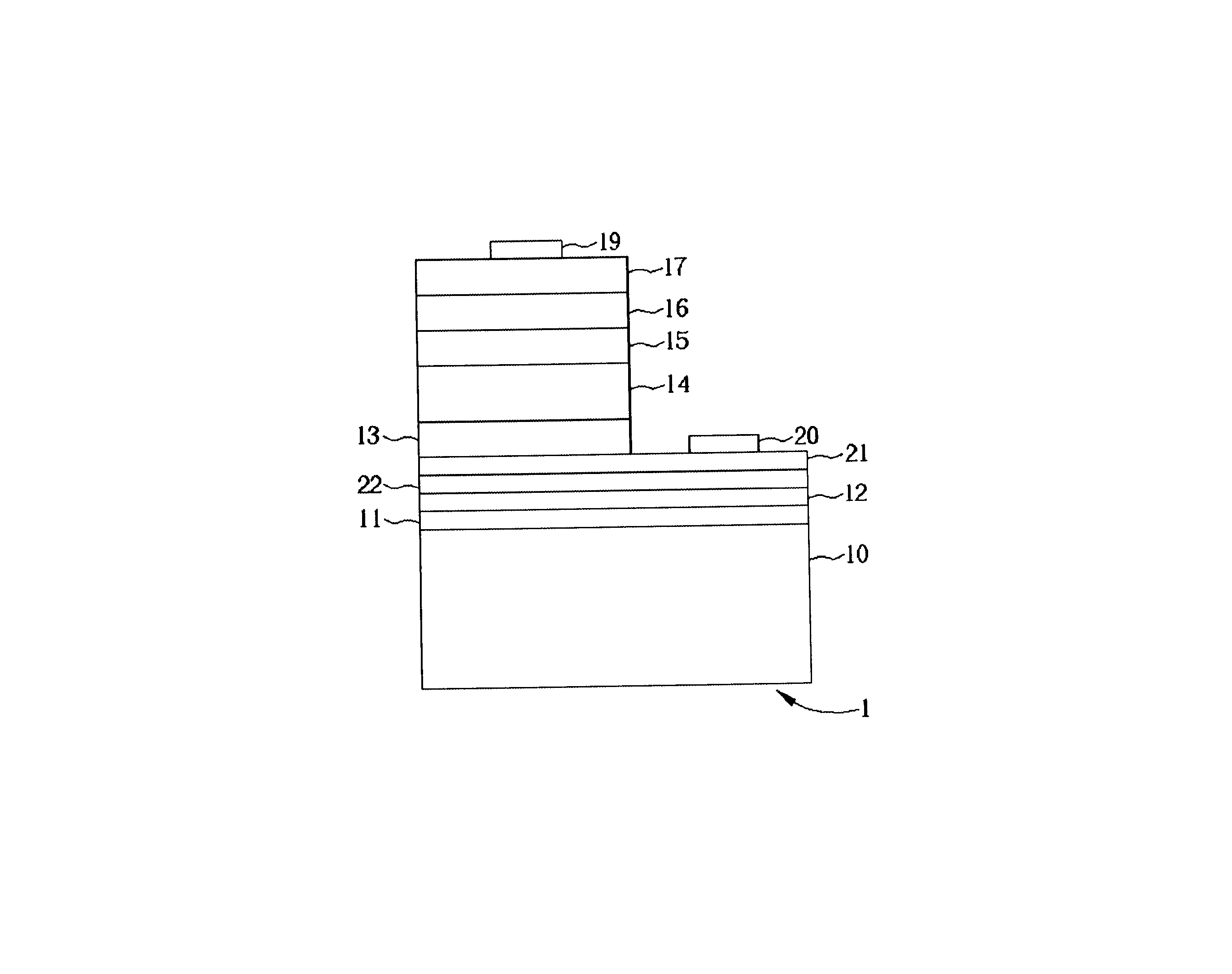
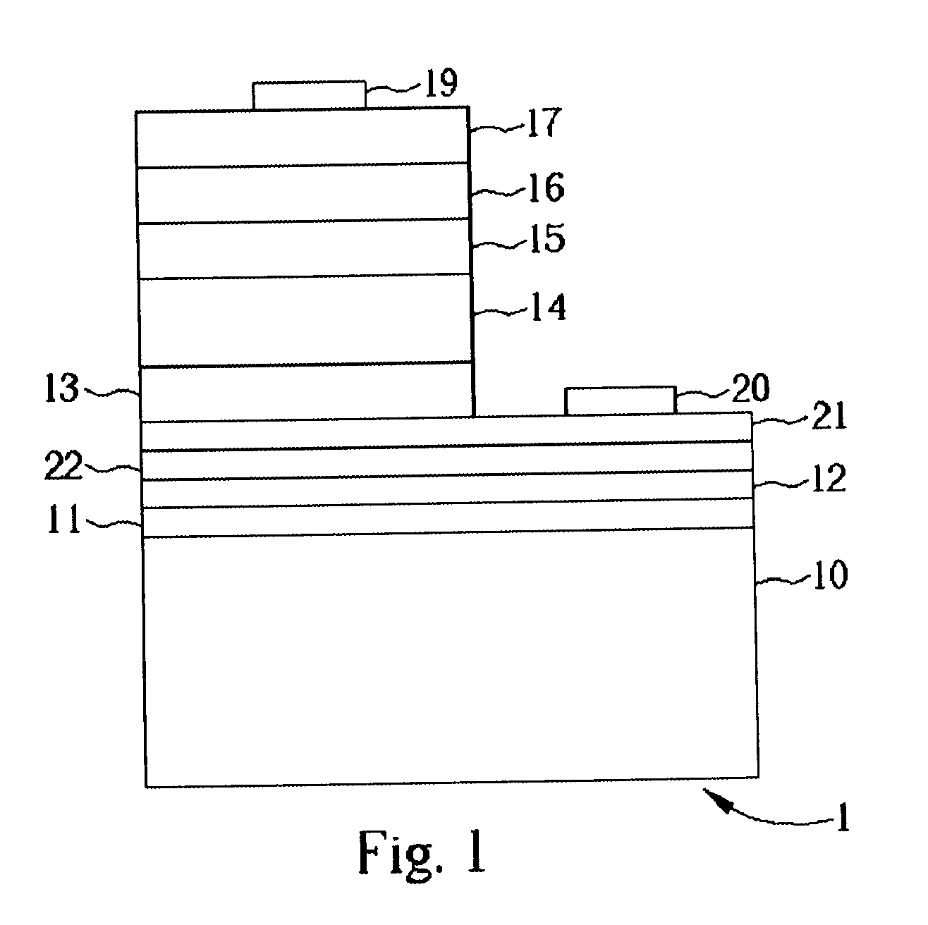
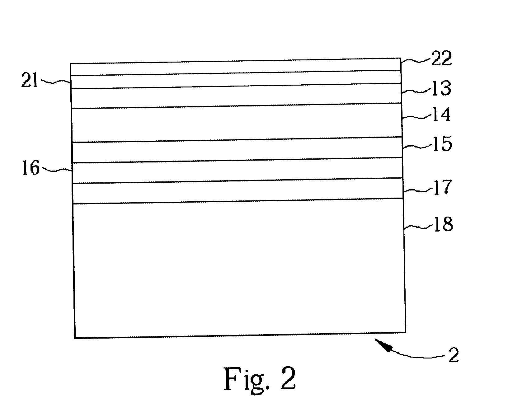
Please refer to FIG. 1. FIG. 1 is a perspective view of a light emitting diode 1 according to the present invention. The light emitting diode 1 comprises a second substrate 10, a first reaction layer 11 formed on the second substrate 10, a transparent adhesive layer 12 formed on the first reaction layer 11, a second reaction layer 22 formed on the transparent adhesive layer 12, and a transparent conductive layer 21 formed on the second reaction layer 22. The transparent conductive layer 21 has a first surface area and a second surface area. The light emitting diode 1 further comprises a first contact layer 13 formed on the first surface area of the transparent conductive layer 21, a first cladding layer 14 formed on the first contact layer 13, an emitting layer 15 formed on the first cladding layer 14, a second cladding layer 16 formed on the emitting layer 15, a second contact layer 17 formed on the second cladding layer 16, a first electrode 19 formed on the second contact layer 1...


PUM


Abstract

A method for forming a light emitting diode includes forming a first stack, forming a second reaction layer over the first stack, forming a second stack, forming a first reaction layer over the second stack, and holding together the first reaction layer and the second reaction layer by means of a transparent adhesive layer. The transparent adhesive layer is formed between the first and second reaction layer, therefore the second reaction layer of the first stack will not come off the first reaction layer of the second stack.

Description

BACKGROUND OF INVENTION1. Field of the InventionThe present invention relates to a light emitting diode, and more particularly, a light emitting diode having an adhesive layer to strengthen the structure of the light emitting diode.2. Description of the Prior ArtLight emitting diodes are widely used in optical displays, laser diodes, traffic lights, data storage devices, communications devices, illumination equipments, and medical equipments. Therefore, enhancing the performance of the light emitting diodes is an important issue in the field of LEDs.Related art teaches a light emitting diode and its manufacturing method in which the light emitting diode is formed by adhering a transparent insulating adhesive layer to an emitting stack and a transparent substrate. The adherence is achieved by Van der Waals forces. However the Van der Waals forces are too weak to hold the emitting stack and the transparent substrate in place. Therefore the emitting stack may come off the transparent s...

Claims


Application Information

Patent Timeline
Patent Type & Authority Patents(United States)
IPC IPC(8): H01L33/00H01L33/30H01L33/34H01L33/42
CPCH01L33/0079H01L33/0093
Inventor HSIEH, MIN-HSUNTSENG, TZU-FENGLIU, WEN-HUANGYEH, TING-WEIWANG, JEN-SHUI
Owner EPISTAR CORP
Learn More