Graphene FET devices, systems, and methods of using the same for sequencing nucleic acids

a technology of graphene transistors and fets, which is applied in the field of field effect transistors, can solve the problems of increasing the amount of sample preparation resources and time, the time and effort that goes into building such full-length genomic sequences and determining, and the method employed in sequencing protocols does not produce full-length dna chromosomal sequences

Active Publication Date: 2017-04-11
CARDEA BIO INC
View PDF603 Cites 37 Cited by
  • Summary
  • Abstract
  • Description
  • Claims
  • Application Information

AI Technical Summary

Benefits of technology

[0018]Provided herein are devices, systems, and methods of employing the same for the performance of genomics and / or bioinformatics analysis. The devices, systems, and methods of the disclosure are directed in part to field effect transistor (FET) sensors, integrated circuits, and arrays employing the same for analyte measurements. The present FET sensors, arrays, and integrated circuits may be fabricated using conventional CMOS processing techniques based on improved FET sensor and array designs that increase measurement sensitivity and accuracy, and at the same time facilitate significantly small sensor sizes and dense gFET sensor based arrays. Particularly, improved fabrication techniques, as well as improved sensor devices, and their use, employing 1D or 2D reaction layers, provide for rapid data acquisition from small sensors to large, including dense arrays of sensors.
[0029]Such FET sensors as herein described may be employed to facilitate DNA hybridization and / or sequencing techniques, such as based on monitoring changes in hydrogen ion concentration (pH), changes in other analyte concentrations, and / or binding events associated with chemical processes (e.g., relating to DNA synthesis), such as within a gated reaction chamber or well of the gFET based sensor, such as proximate the reaction zone(s). For example, the chemically-sensitive field effect transistor may be configured as a CMOS biosensor and / or may be adapted to increase the measurement sensitivity and / or accuracy of the sensor and / or associated array(s), such as by including one or more surfaces or wells having a surface layered with a 1D and / or 2D and / or 3D material, a dielectric or reaction layer, a passivation layer, and the like. In particular instances, the increased sensitivity of the sensors may, in part, be due to the presence of the presence of the 1D or 2D material, and / or further enhanced by its relationship to one or more of the reaction and / or passivation layers, which in turn allows for smaller sensor configurations, therefore smaller channels and / or gates, and thus a greater density of sensors and / or arrays.
[0030]For instance, in a particular embodiment, a chemically-sensitive graphene containing field effect transistor (gFET), such as a gFET having a CMOS structure is provided, where the gFET sensor, e.g., biosensor, may include an oxide and / or passivation layer, such as a layer that is disposed on the surface of the well or chamber so as to increase the measurement sensitivity and / or accuracy of the sensor and / or associated array(s). The oxide layer, when present, may be composed of an aluminum oxide, a silicon oxide, a silicon dioxide, and the like. More particularly, the oxide and / or passivation layers may have a suitable thickness such as of from about 100 nm to about 75 nm, such as from about 50 nm to about 30 nm, from about 40 nm to about 25 nm, such as from about 20 nm to about 10 nm or 9 nm or less, respectively.
[0045]Accordingly, in particular embodiments, a further structured layer, e.g., a secondary or tertiary structure, may also be provided, such as where the further structured layer may be included and / or present within the well or chamber, such as to enhance the ability of the processor to determine the difference between the current and / or voltages as well as their respective associated curves. More particularly, the additional structure may include an ion-selective permeable membrane, such as an ion-selective permeable membrane that allows ions of interest to pass through the membrane while blocking other ions, such as to enhance the ability of the processor to determine the difference between the reference I-V or I-Vg curve and the chemical reaction I-V or I-Vg curve, and thus enhance the ability of the processor to detect a desired chemical reaction. In various instances, the FET may be configured such that the I-V or I-Vg curve(s) may be shifted so as to better respond to, detect, and / or otherwise determine a biological compound and / or a chemical reaction, such as a biological compound and / or a chemical reaction occurring on the 1D or 2D, e.g., graphene, surface of the chemically-sensitive field effect transistor. In particular instances, the ion-selective permeable membrane may include a 2D transistor material, e.g., graphene, which may or may not be electrically connected to the source and / or drain layer and / or channel.
[0047]In particular instances, an additional material, e.g., HMDS, may be included so as to manage the interaction of the chamber and / or channel and / or associated oxide layer and / or underlying 1D or 2D or 3D transistor layer. For instance, a chemically-sensitive field effect transistor of the disclosure may include a secondary or tertiary structure that includes a 2D transistor channel or surface which may include an ion-sensitive material over the channel or surface. In such an instance, the material may be sensitive to ions that are different from the ions associated with the biological molecule or chemical reaction that is to be detected. Particularly, in some instances, the action of sensing ions that are different from the ions associated with the biologics and / or chemical reactions that are to be detected allows the processor to filter out the signal from the unwanted ions from the signal of the ions of interest.
[0051]The use of electrophoresis and / or magnetism allows for thinner reaction location structures. In particular instances, therefore, an electric and / or magnetic field generator may be configured for drawing and / or positioning a microbead within the well structure, such as in proximity to a channel or chamber of the device, and in other instances, the electric and / or magnetic field generator may be configured for reversing the electrical and / or magnetic field so as to repulse the microbead from the reaction location, channel, and / or chamber. In various instances, an array of reaction locations may be provided each having a magnet that allows for selective filling of the reaction locations with different numbers and / or types of microbeads, such as at select reaction locations. In such an instance, multiple electric and / or magnetic field generators for selective filling of reaction locations, e.g., wells.

Problems solved by technology

For example, a central challenge in DNA sequencing is assembling full-length genomic sequence data, e.g., of chromosomal sequences, from a sample of genetic material obtained from a subject.
In particular, the methods employed in sequencing protocols do not produce full-length chromosomal sequences of the sample DNA.
However, as the human genome is comprised of approximately 3.1 billion base pairs, and as each sequence fragment is typically only from about 100 to 500 to 1,000 nucleotides in length, the time and effort that goes into building such full length genomic sequences and determining the variants therein is quite extensive, often requiring the use of several different computer resources applying several different algorithms over prolonged periods of time.
To perform this over-coverage, e.g., using PCR, may require increased sample preparation resources and time, and therefore be more expensive, but it often gives an enhanced probability of the end result being more accurate.
This greatly accelerates the synthesis process.
However, in part, due to the need for the use of optically detectable, e.g., fluorescent, labels in the sequencing reactions being performed, the required instrumentation for performing such high throughput sequencing is bulky, costly, and not portable.
The promise of this idea has not been realized commercially due to the fundamental limits of applying a metal oxide semiconductor field effect transistor, or MOSFET, as a biosensor.
A particular limitation, however, includes a lack of sensor sensitivity and signal to noise characteristics as the semiconductor node scales down to lower geometries of the transistor (gate length).
However, this requires short gates and fast carriers in the channel.
Unfortunately, FETs with short gates frequently suffer from degraded electrostatics and other problems (collectively known as short channel effects), such as threshold-voltage roll-off, drain-induced barrier lowering, and impaired drain-current saturation, results in a decrease in sensor sensitivity.
Nevertheless, these effects make the use of such technologies difficult to employ in sequencing reactions.

Method used


Image

  • Graphene FET devices, systems, and methods of using the same for sequencing nucleic acids
  • Graphene FET devices, systems, and methods of using the same for sequencing nucleic acids
  • Graphene FET devices, systems, and methods of using the same for sequencing nucleic acids

Examples


Embodiment Construction

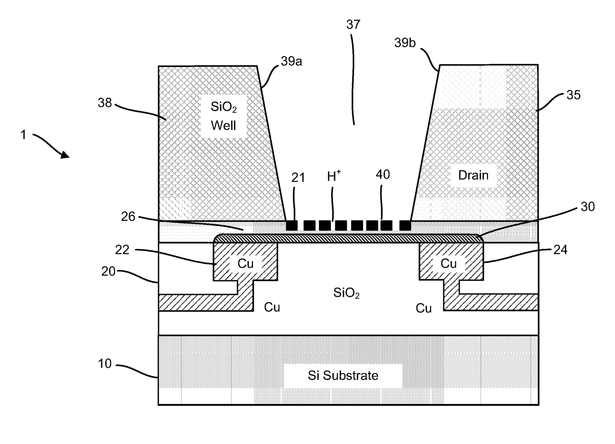
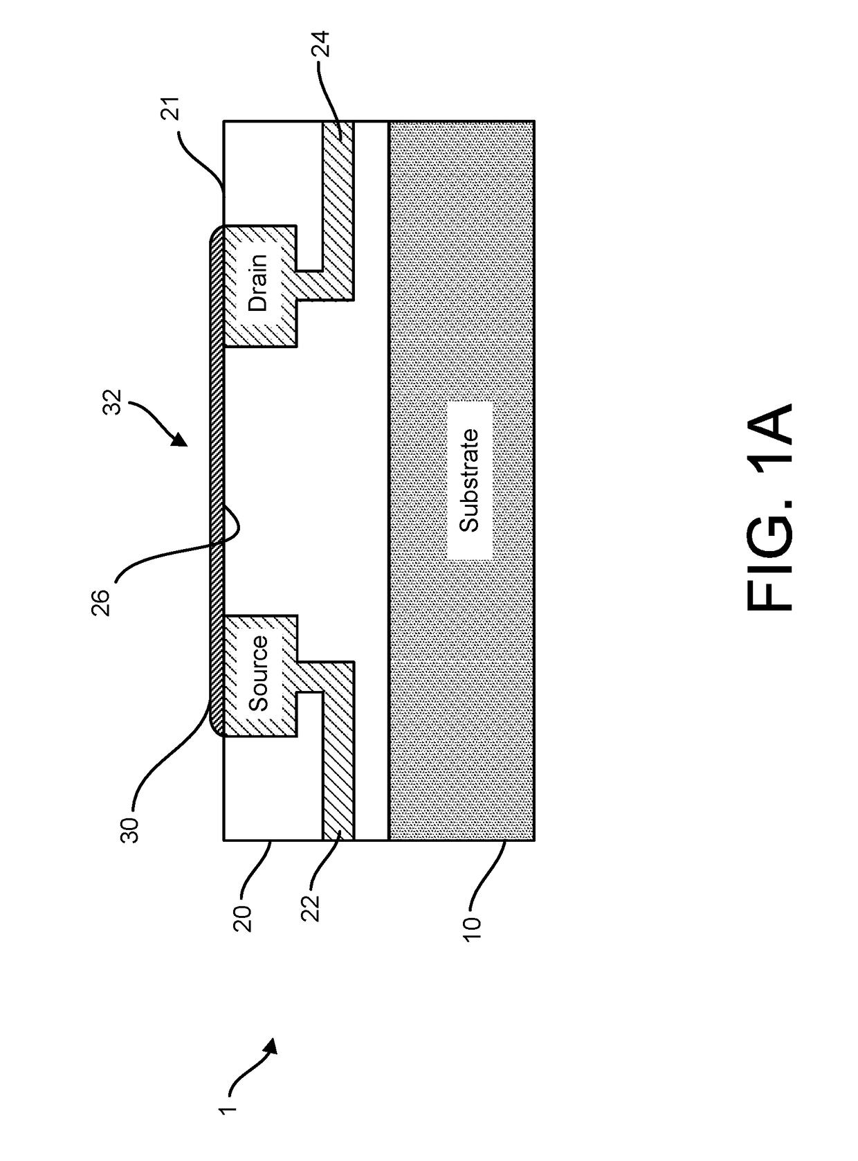
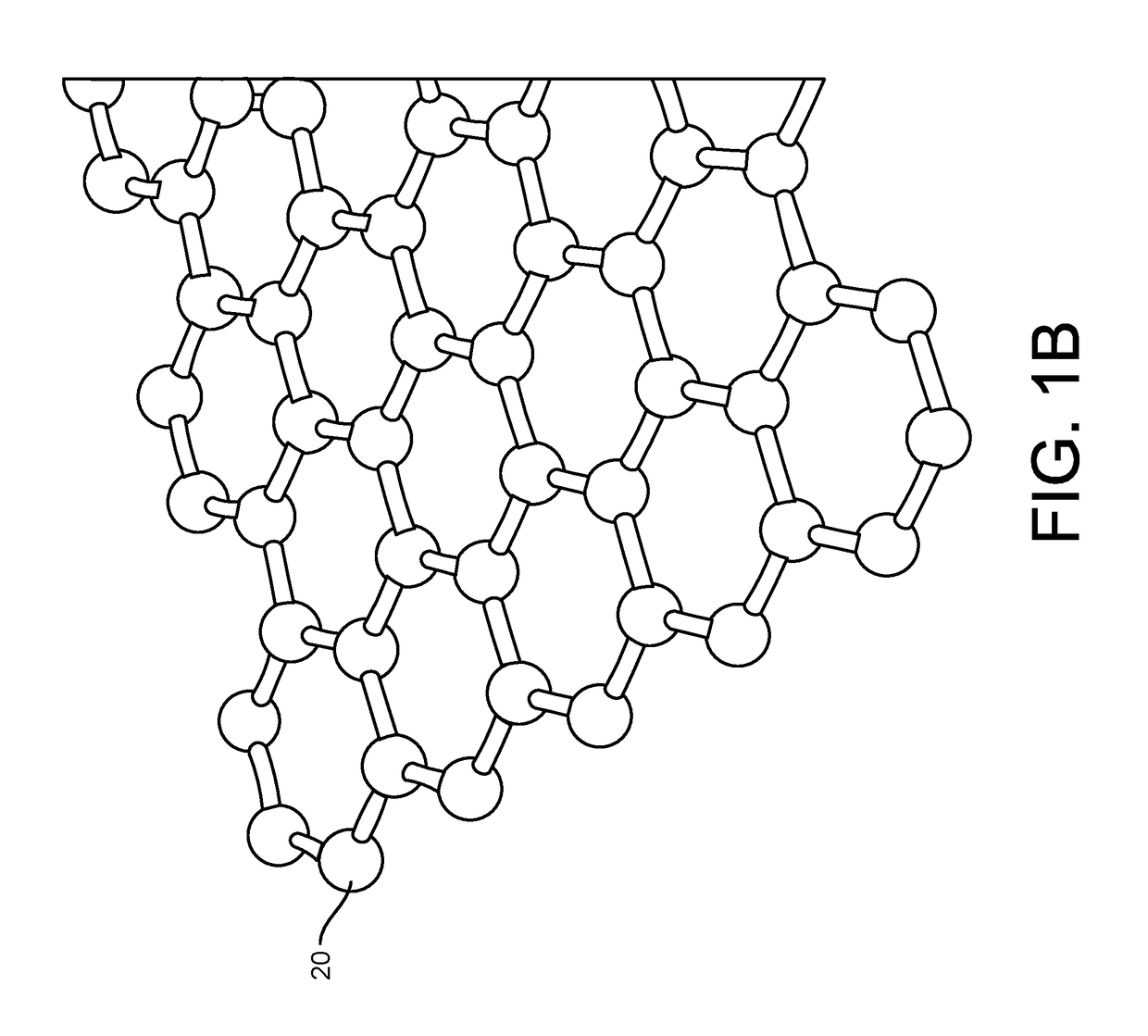
[0110]Accordingly, provided herein are devices, systems, and methods of employing the same for the performance of one or more chemical and / or bioinformatics analysis operations. Particularly, the devices, systems, and methods of the disclosure are directed in part to 1D, 2D, or 3D field effect transistor (FET) sensors, integrated circuits, and arrays employing the same for analyte measurements. The present FET sensors, arrays, and integrated circuits may be fabricated using conventional CMOS processing techniques based on improved 1D, 2D, or 3D FET sensor and array designs that increase measurement sensitivity and accuracy, and at the same time facilitate significantly small sensor sizes and dense sensor array designs.

[0111]More particularly, such improved fabrication techniques employing 1D, 2D, e.g., graphene, or 3D materials as a reaction layer provide for rapid data acquisition from small sensors to large and dense arrays of sensors. Such arrays may be employed to detect the pre...


PUM

PropertyMeasurementUnit
lengthaaaaaaaaaa
lengthaaaaaaaaaa
widthaaaaaaaaaa

Abstract

Provided herein are devices, systems, and methods of employing the same for the performance of bioinformatics analysis. The apparatuses and methods of the disclosure are directed in part to large scale graphene FET sensors, arrays, and integrated circuits employing the same for analyte measurements. The present GFET sensors, arrays, and integrated circuits may be fabricated using conventional CMOS processing techniques based on improved GFET pixel and array designs that increase measurement sensitivity and accuracy, and at the same time facilitate significantly small pixel sizes and dense GFET sensor based arrays. Improved fabrication techniques employing graphene as a reaction layer provide for rapid data acquisition from small sensors to large and dense arrays of sensors. Such arrays may be employed to detect a presence and / or concentration changes of various analyte types in a wide variety of chemical and / or biological processes, including DNA hybridization and / or sequencing reactions. Accordingly, GFET arrays facilitate DNA sequencing techniques based on monitoring changes in hydrogen ion concentration (pH), changes in other analyte concentration, and / or binding events associated with chemical processes relating to DNA synthesis within a gated reaction chamber of the GFET based sensor.

Description

CROSS-REFERENCE TO RELATED APPLICATIONS[0001]This application claims the benefit of priority to U.S. Provisional Application Ser. No. 62 / 130,598, filed on Mar. 9, 2015; U.S. Provisional Application Ser. No. 62 / 130,594, filed on Mar. 9, 2015; U.S. Provisional Application Ser. No. 62 / 130,601, filed on Mar. 9, 2015; U.S. Provisional Application Ser. No. 62 / 130,621, filed on Mar. 10, 2015; and a continuation in part of U.S. application Ser. No. 14 / 963,253, filed on Dec. 9, 2015, which in turn claims benefit of U.S. Provisional Application Ser. No. 62 / 094,016, filed on Dec. 18, 2014.FIELD OF THE DISCLOSURE[0002]The present disclosure relates, generally, to field effect transistors, such as integrated field-effect devices, systems including the devices, and methods of using the same for the analysis of biological and / or chemical materials, such as for molecular, e.g., nucleic acid, analysis and / or sequencing. More specifically, the present disclosure relates to field effect transistors ha...

Claims


Application Information

Patent Timeline
Patent Type & Authority Patents(United States)
IPC IPC(8): H01L29/66B01L3/00H01L29/16C12Q1/68G01N27/414H01L27/085H01L29/24H01L29/10
CPCG01N27/414B01L3/502715C12Q1/6874G01N27/4145G01N27/4146G01N27/4148H01L27/085H01L29/1029H01L29/1606H01L29/24B01L2300/0627B01L2300/0858B01L2300/0887B01L2300/12B01L3/502761C12Q1/6869
Inventor VAN ROOYEN, PIETERLERNER, MITCHELLHOFFMAN, PAUL
Owner CARDEA BIO INC
Why Eureka
Try Eureka