Method to control critical dimension of a hard masked pattern

a technology of microelectronic integrated circuit and polysilicon gate, which is applied in the direction of basic electric elements, electrical apparatus, and devices based on varying gate lengths, can solve the problems of inability to control the inability to provide details about the amount of cd reduction in nm, so as to reduce cd, reduce cd, and control the effect of treatmen

Inactive Publication Date: 2005-04-12
TAIWAN SEMICON MFG CO LTD
View PDF13 Cites 40 Cited by
  • Summary
  • Abstract
  • Description
  • Claims
  • Application Information

AI Technical Summary

Benefits of technology

Referring to FIG. 1G, the pattern in hard mask 120 with a CD L3 is etch transferred by a conventional method into gate layer 110 to form a gate length L3. The hard mask 120 may be removed by a standard method after the gate 110 is formed or may remain in the device. The etch may be optimized so that CD (L3) is transferred into gate layer 110 with little or no further etch bias. Therefore, the advantage of the present invention is that it produces a final gate length which can be controlled to within 3 to 5 nm of a target value for the particular device. Another feature of this invention is that a CD (L3) can be produced that is smaller than the photoresist CD (L1) or by trimming a photoresist image with a dry etch to give a reduced CD (L2).
further etch bias. Therefore, the advantage of the present invention is that it produces a final gate length which can be controlled to within 3 to 5 nm of a target value for the particular device. Another feature of this invention is that a CD (L3) can be produced that is smaller than the photoresist CD (L1) or by trimming a photoresist image with a dry etch to give a reduced CD (L2).
In another embodiment where the hard mask is silicon oxynitride or silicon nitride, the treatment steps described above for the oxide hard mask are preceded by a wet etch step in buffered HF (BHF). Substrate 80 is dipped in a BHF solution (1:100 HF / water) for a period of 5 to 60 seconds at a temperature range of from 20° C. to 50° C. and preferably at 23° C. A typical etch rate for the BHF dip is about 0.05 nm per second. During this dip, the BHF also helps to remove any plasma etch residues from a previous step. A oxynitride or nitride etch rate in BHF is independent of life count. The substrate 80 is normally rinsed with DI water and dried before proceeding to the next treatment.
The substrate 80 is then dipped in the SPM solution described previously for a period of 0 to about 3600 seconds at a temperature in the range of about 60° C. to about 150° C., and preferably in the range of 125° C. to 130° C. The ratio of H2SO4 to H2O2 is preferably 4:1 but can be greater than 6:1. In this case the SPM treatment is believed to have a minor role in the lateral etch and assists primarily in cleaning the surface of any plasma etch residue. The SPM temperature, time of dip and ratio of H2SO4 to H2O2 may be altered from one wafer to the next in order to control the effectiveness of the treatment since the inventors have found that the etch rate linearly increases with SPM life count.
Next, substrate 80 is dipped in an APM solution described previously for a period of 0 to about 600 seconds at a temperature in the range of about 15° C. to about 75° C., and preferably in the range of 35° C. to 50° C. The ratio of NH4OH:H2O2:H2O is from 1:1:1 to about 1:5:125, respectively, and preferably in the range of 1:2:50 to about 1:4:20. In this case, the etch rate the oxynitride or nitride hard mask 120 is independent of life count of the APM solution. FIG. 2 demonstrates the linear relationship of dip time in the APM solution to reduction in CD for an oxynitride hard mask. On average, the CD becomes 6 Angstroms (0.6 nm) smaller per 30 second dip time. The overall reduction in CD (L3-L2) is in the range of 0 to 12 nm, and preferably from 0 to 5 nm. The method of this embodiment is an advantage over prior art in that the size of a nitride or oxynitride hard mask can be trimmed from a dimension L2 to L3 while maintaining L3 within 3 to 5 nm of a target value. Furthermore, the etch treatment cleans the substrate unlike the case where a plasma etch is the final step in trimming a CD and subsequent cleaning processes are required.
Referring to FIG. 1H, the process may be further comprised of forming a transistor 150 between STI regions 90 by removing exposed regions of gate dielectric layer 100, forming lightly doped source / drain (S / D) regions 160 in the substrate, forming spacers 170 on the sidewalls of gate electrode 110 and on dielectric layer 100, forming heavily doped S / D regions 180 in substrate 80, and performing a silicidation to produce silicide regions 190 on gate electrode 110 and on heavily doped S / D regions 180. Since the gate length L3 has been tightly controlled to within 3 to 5 nm of a target specification, the resulting transistor provides optimum performance.

Problems solved by technology

However, if the hard mask etch is not controlled to produce CD values within a tight specification range, then the devices based on varying gate lengths will still have an unacceptable range of performance.
However, no details are provided about the amount of CD reduction in nm or how well the CD reduction is controlled.

Method used


Image

  • Method to control critical dimension of a hard masked pattern
  • Method to control critical dimension of a hard masked pattern
  • Method to control critical dimension of a hard masked pattern

Examples


example 1

Wet Etch Process of an Oxide Hard Mask

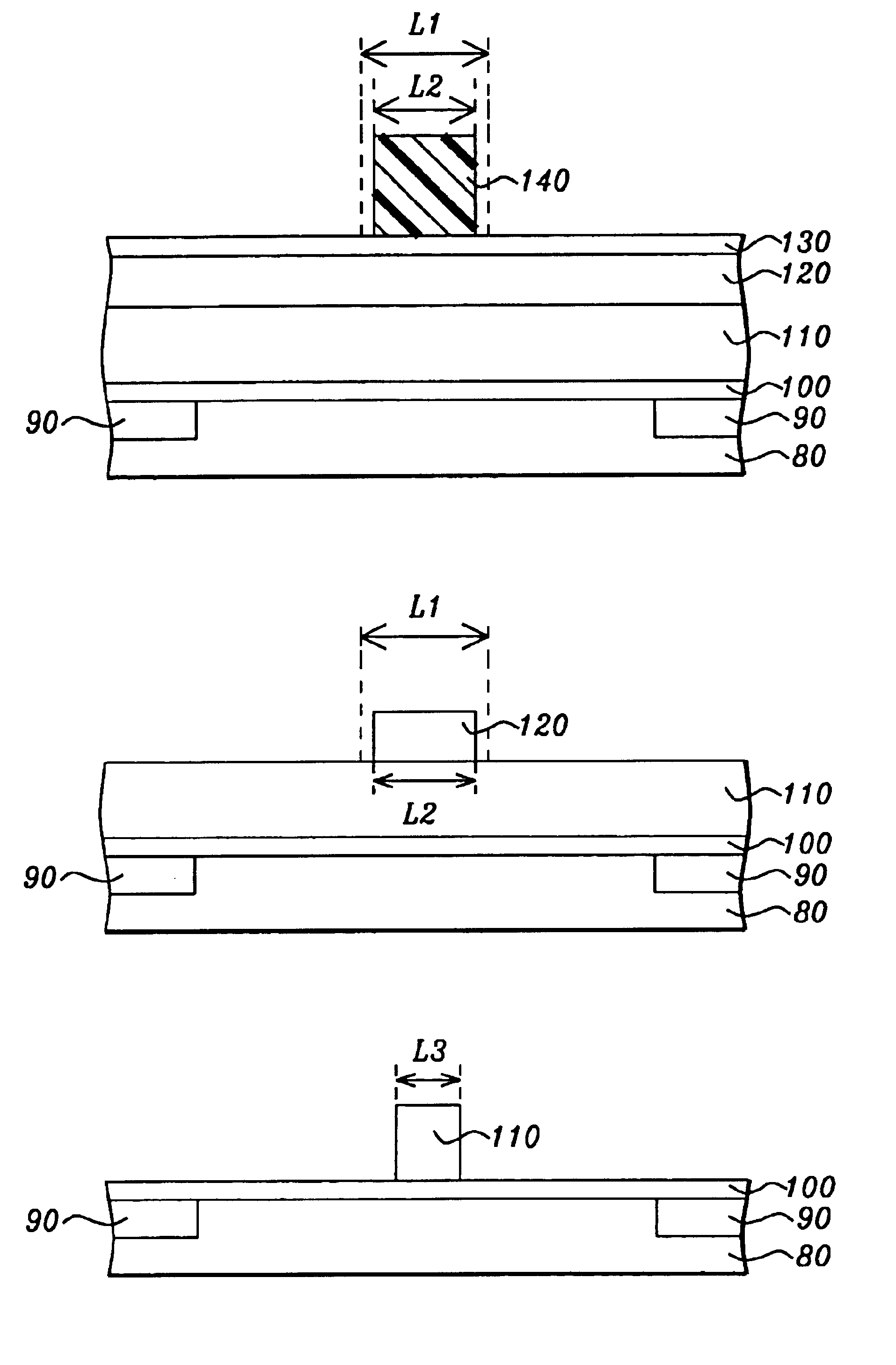
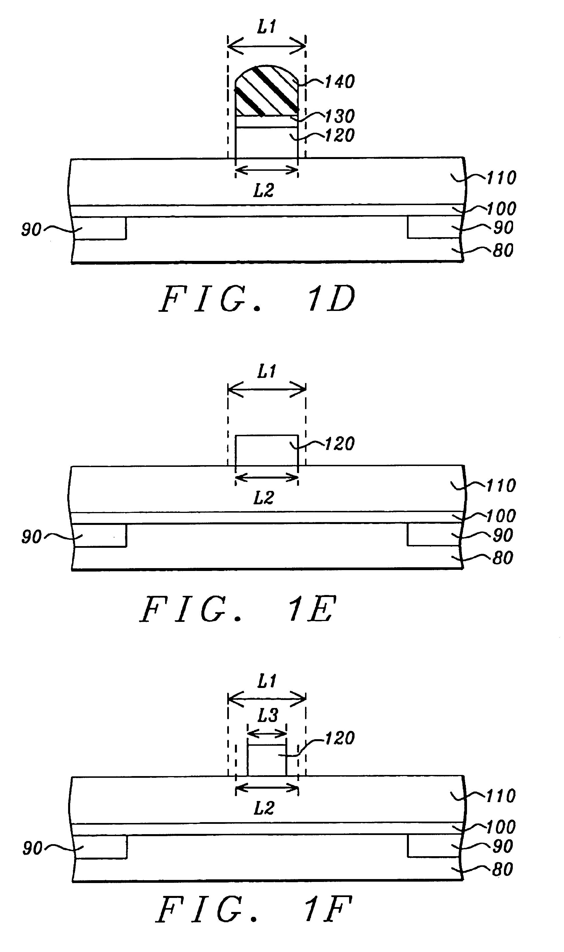
A patterned substrate that was processed through the etch transfer step into a 500 Angstrom thick oxide hard mask as shown in FIG. 1E was taken through the following steps. A substrate with a hard mask CD L2 of 149 nm was dipped in an SPM solution with a H2SO4H2O2 ratio of 4:1 at 130° C. for 1800 seconds. This process was repeated two more times at the same concentration, dip time and temperature. The substrate was rinsed with 800 ml of deionized water and dried by a Maragoni dryer for 600 seconds. The resulting hard mask CD (L3) was measured to be 147 nm. The substrate was then dipped in an APM solution with a NH4OH: H2O2: H2O ratio of 1:4:20 at 50° C. for 60 seconds and rinsed with 800 ml of deionized water and dried by a Maragoni dryer for 600 seconds. The resulting hard mask CD (L3) was 147 nm with a CD variation of + / −2 nm. The substrate was then etched with a standard polysilicon gate dry etch to transfer the pattern with dimension L3 into...

example 2

Wet Etch Process of an Oxynitride Hard Mask

A patterned substrate that was processed through the etch transfer step into an 500 Angstrom thick oxynitride hard mask 120 as shown in FIG. 1E was taken through the following steps. The substrate with a hard mask CD L2 of 150 nm was dipped in a buffer HF (BHF) solution (1:100 HF :H2O) at 23° C. for 15 seconds and then rinsed with 800 ml of DI water and dried by a Maragoni dryer for 600 seconds. The substrate was then dipped in an SPM solution with a H2SO4: H2O2 ratio of 4:1 at 50° C. for 1800 seconds. The SPM treatment was repeated two more times at the same concentration, dip time and temperature. The wafer was rinsed with 800 ml of deionized water and dried by a Maragoni dryer for 600 seconds. The resulting hard mask CD (L3) was measured to be 149 nm. The substrate was next dipped in an APM solution with a NH4OH: H2O2: H2O ratio of 1:4:20 at 50° C. for 180 seconds and rinsed with 800 ml of DI water and dried by a Maragoni dryer for 600 s...


PUM

PropertyMeasurementUnit
thicknessaaaaaaaaaa
thicknessaaaaaaaaaa
temperatureaaaaaaaaaa

Abstract

A method of reducing the critical dimension (CD) of a hard mask by a wet etch method is described. An oxide hard mask is treated with a H2SO4/H2O2 (SPM) solution followed by treatment with a NH4OH/H2O2/H2O (APM) solution to trim the CD by 0 to 20 nm. With nitride or oxynitride hard masks, a buffered HF dip is inserted prior to the SPM treatment. For oxide hard masks, the SPM solution performs the etch while APM solution assists in removing plasma etch residues. With oxynitride hard masks, the APM performs the etch while BHF and SPM solutions remove plasma etch residues. The hard mask pattern can then be transferred with a dry etch into an underlying polysilicon layer to form a gate length of less than 150 nm while controlling the CD to within 3 to 5 nm of a targeted value.

Description

FIELD OF THE INVENTIONThe invention relates to a method of forming a polysilicon gate in a microelectronic integrated circuit. More particularly, the present invention is directed to the method of controllably wet etching to reduce a critical dimension (CD) of a hard mask.BACKGROUND OF THE INVENTIONOne of the key steps in the manufacture of a semiconductor device is formation of a gate electrode which will hereafter be referred to as the gate. The gate length which is the horizontal measurement between vertical sidewalls of the gate is typically one of the smallest dimensions in the device. The gate length is a critical dimension (CD) since the performance of the resulting device is related to its size. Gate lengths of less than 100 nm are currently required to meet the demand for a faster transistor speed in advanced technologies. A high performance also requires that the gate length or CD must be controlled within a tight specification, typically within a 3 to 5 nm variation acros...

Claims


Application Information

Patent Timeline
Patent Type & Authority Patents(United States)
IPC IPC(8): H01L21/02H01L21/302H01L21/033H01L21/28H01L21/311H01L21/3213
CPCH01L21/0338H01L21/28123H01L21/32139H01L21/31111Y10S438/947
Inventor TSAI, CHAO-TZUNGWU, JIA-SHENGFANG, FUXUAN
Owner TAIWAN SEMICON MFG CO LTD
Why Eureka
Try Eureka