Package structure of light emitting diode

a technology of light-emitting diodes and packaging materials, which is applied in the direction of basic electric elements, electrical apparatus, and semiconductor devices, can solve the problems of packaging materials, reducing the brightness or accelerating the aging of devices, and easy degeneration or fragility of resin materials exposed to ultraviolet ligh

Active Publication Date: 2005-04-19
NYTELL SOFTWARE LLC
View PDF1 Cites 110 Cited by
  • Summary
  • Abstract
  • Description
  • Claims
  • Application Information

AI Technical Summary

Benefits of technology

[0008]In order to provide solutions for the aforementioned problems, the present invention provides a LED package structure including a housing of a silicon optical bench (SiOB). The present invention also provides an LED package structure including a transparent plate made of glass or crystal materials. The package structure of the present invention does not use any resin molding materials, so that prior art problems of degeneration or friability can be avoided. Furthermore, the package structure of the present invention ensures that the LED generates unicolor light without color aberration.
[0010]The package structure of the present invention employs the transparent plate made of glass or a crystal material, thus avoiding using any resin molding materials. Therefore, the present invention can avoid prior art problems of degeneration or friability resulting from exposure to light.
[0011]Alternatively, the angle between the bottom surface and the sidewall of the trench of the package housing can be designed to be larger than 90 degrees. A metallic reflective layer is coated over the sidewalls and the bottom surface of the trench, except for those regions occupied by the leads and the die. During the operation of the LED, visible light is generated by the LED chip by applying voltages of different polarity, and the metallic reflective layer can reflect the light to emit through the transparent plate, thus increasing illuminance efficiency.

Problems solved by technology

However, the resin materials when exposure to UV light can easily become degenerated or fragile.
Therefore, if UV LEDs or other LEDs of near UV wavelength are fitted in this conventional LED package structure, the emitting UV or near UV light may damage the packaging materials, thus lowering the brightness or accelerating aging of the device.
As a result, the application of certain types of LEDs is severely limited by using this type of package structure.

Method used


Image

  • Package structure of light emitting diode
  • Package structure of light emitting diode
  • Package structure of light emitting diode

Examples


Embodiment Construction

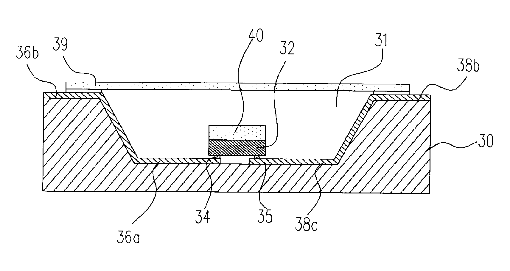
[0019]The present invention relates to a package structure for a light emitting diode (LED). The package structure of this invention includes a package housing having a trench and at least two leads. For both leads, one end of the lead is disposed on the bottom surface of the trench, while the other end of the lead reaches out and is disposed on the surface of the housing. The package structure includes at least a die or an LED chip disposed on the bottom surface of the trench, while two electrodes of the die are respectively connected to the ends of two leads on the bottom surface of the trench. Then, a transparent plate of glass or crystal materials is mounted and connected to the housing by anodic bonding or glue bonding, to seal the trench, while the other ends of leads are exposed on the surface of the housing without being covered by the transparent plate. According to the embodiments of this invention, the housing may, but not limited to, be a silicon optical bench (SiOB), wh...


PUM


Abstract

The present invention relates to a package structure for a light emitting diode (LED). The LED package structure of this invention includes a package housing having at least a trench and at least two leads. The package structure includes at least a die or an LED chip disposed on the bottom surface of the trench, while two electrodes of the die are respectively electrically connected to the ends of two leads on the bottom surface of the trench. A transparent plate of glass or crystal materials is mounted and connected to the housing by anodic bonding or glue bonding, to seal the trench, while the other ends of leads are exposed on the surface of the housing without being covered by the transparent plate.

Description

BACKGROUND OF INVENTION[0001]1. Field of Invention[0002]The present invention relates to a package structure of a light emitting diode. More particularly, the present invention relates to a package structure of a light emitting diode having a package housing of a silicon optical bench.[0003]2. Description of Related Art[0004]The mechanism of light emitting diodes (LEDs) relates to light emission resulting from the released energy during the recombination of electrons and holes in the semiconductor materials. Due to numerous advantages of the light emitting diodes including miniature sizes, durability, low-driven voltages, low electricity consumption, fast response speed and good monochromatism, they are widely applied as light emitting elements in various electronic products, display panels and communication products.[0005]For the light emitting diodes of various types, the light emitting diodes can be categorized as visible light LEDs and non-visible light (infrared light) LEDs bas...

Claims


Application Information

Patent Timeline
Patent Type & Authority Patents(United States)
IPC IPC(8): H01L31/12H01L27/15H01L33/00H01L33/48H01L33/56H01L33/58
CPCH01L33/56H01L33/486H01L33/58H01L2924/12041H01L2224/48247H01L2224/48091H01L2924/00014
Inventor TING, CHU-CHI
Owner NYTELL SOFTWARE LLC
Why Eureka
Try Eureka