Methods and apparatus for providing an antifuse function

a technology of anti-fuse latch and anti-fuse, which is applied in the direction of electrical apparatus, semiconductor devices, semiconductor/solid-state device details, etc., can solve the problems of fusing latch margin and attendant poor performan

Inactive Publication Date: 2005-04-19
SAMSUNG ELECTRONICS CO LTD +1
View PDF5 Cites 33 Cited by
  • Summary
  • Abstract
  • Description
  • Claims
  • Application Information

AI Technical Summary

Benefits of technology

[0016]In accordance with one or more further aspects of the present invention, a method of forming an antifuse includes forming a semiconductor substrate having an active area circumscribed by a shallow trench isolation (STI) boundary, wherein the active area of the semiconductor substrate includes a longitudinal member and a plurality of finger portions extending transversely to the longitudinal member; disposing a dielectric on or above the semiconductor substrate; forming a gate conductor having a longitudinal member and a plurality of finger portions extending transversely to the longitudinal member, such that the gate conductor is disposed on or above the dielectric and above the semiconductor substrate, and such that at least some of the finger portions of the gate conductor overly at least some portions of the STI boundary; coupling a first terminal to the gate conductor; and coupling a second terminal to the semiconductor substrate.

Problems solved by technology

Unfortunately, this rather large range of resistance significantly reduces the fuse latch margin and results in an attendant poor performance.

Method used


Image

  • Methods and apparatus for providing an antifuse function
  • Methods and apparatus for providing an antifuse function
  • Methods and apparatus for providing an antifuse function

Examples


Embodiment Construction

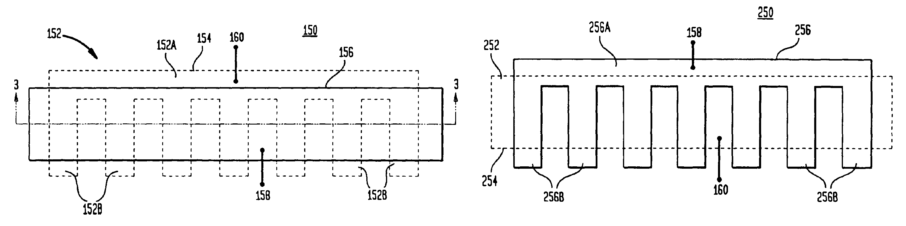
[0025]Referring now to the drawings wherein like numerals indicate like elements, there is shown in FIG. 1 a top view of an antifuse element 100. The antifuse element 100 includes a substrate having an active area 102 that is circumscribed by a shallow trench isolation (STI) boundary 104. A gate conductor 106 is disposed above the semiconductor substrate and entirely within the STI boundary 104. A dielectric layer (not shown) is disposed between the active area 102 of the semiconductor substrate and the gate conductor 106. Although not shown, a first terminal is coupled to the gate conductor 106 and a second terminal is coupled to the active area 102 of the semiconductor substrate. When an external voltage is applied between the gate conductor 106 and the active area 102 of the semiconductor substrate, the dielectric layer breaks down and one or more electrical connections between the gate conductor 106 and the active area 102 of the semiconductor substrate are obtained.

[0026]In thi...


PUM


Abstract

Methods and apparatus for providing an antifuse are disclosed, where the antifuse includes a semiconductor substrate having an active area circumscribed by a shallow trench isolation (STI) boundary; a gate conductor disposed above the semiconductor substrate and overlying at least a portion of the STI boundary; a dielectric disposed between the semiconductor substrate and the gate conductor; a first terminal coupled to the gate conductor; and a second terminal coupled to the semiconductor substrate, wherein a breakdown of the dielectric causes electrical connections between regions of the gate conductor and regions of the active area including substantially near the STI boundary.

Description

BACKGROUND OF THE INVENTION[0001]The present invention relates to methods and apparatus for improving the resistance between a gate conductor and an active area of an antifuse programming elements.[0002]In integrated circuit manufacturing, it is desirable to provide the ability to select various circuit components and / or circuits from an array. For example, redundant parallel circuits may be formed in an integrated circuit and, after testing a given circuit to ensure that it functions properly, the other parallel circuits may be removed. Conversely, a parallel circuit may also be added. While fuses are used to remove unwanted circuit components or circuits, antifuses are employed to add circuits or circuit components. Antifuse elements are normally electrically open, or non-conducting, and are programmable to permit a user to “blow” the element in order to create a useable short circuit.[0003]Various conventional antifuses exist in the art in order to provide the ability to select c...

Claims


Application Information

Patent Timeline
Patent Type & Authority Patents(United States)
IPC IPC(8): H01L23/525H01L23/52
CPCH01L23/5252H01L2924/0002H01L2924/00
Inventor BRINTZINGER, AXELRADENS, CARLTONTI, WILLIAM
Owner SAMSUNG ELECTRONICS CO LTD
Why Eureka
Try Eureka