MOSFET performance improvement using deformation in SOI structure

a technology of soi structure and mosfet, which is applied in the direction of semiconductor devices, basic electric elements, electrical equipment, etc., can solve the problems of increasing manufacturing costs and degrading the performance of p-type devices

Inactive Publication Date: 2005-05-03
GLOBALFOUNDRIES INC
View PDF68 Cites 61 Cited by
  • Summary
  • Abstract
  • Description
  • Claims
  • Application Information

AI Technical Summary

Problems solved by technology

However, the same stress component, either tensile or compressive stress, discriminatively affects the characteristics of an N type device and a P type device.
For example, when tensile stress is applied to a device in the direction of current flow, the performance of an N type device is enhanced but the performance of a P type device is degraded.
While these methods enables selectively applying tensile stress to the N type device and compressive stress to the PFET device along the longitudinal direction, they require more complicated processing steps and specific materials, thereby increasing manufacturing costs.

Method used


Image

  • MOSFET performance improvement using deformation in SOI structure
  • MOSFET performance improvement using deformation in SOI structure
  • MOSFET performance improvement using deformation in SOI structure

Examples


Embodiment Construction

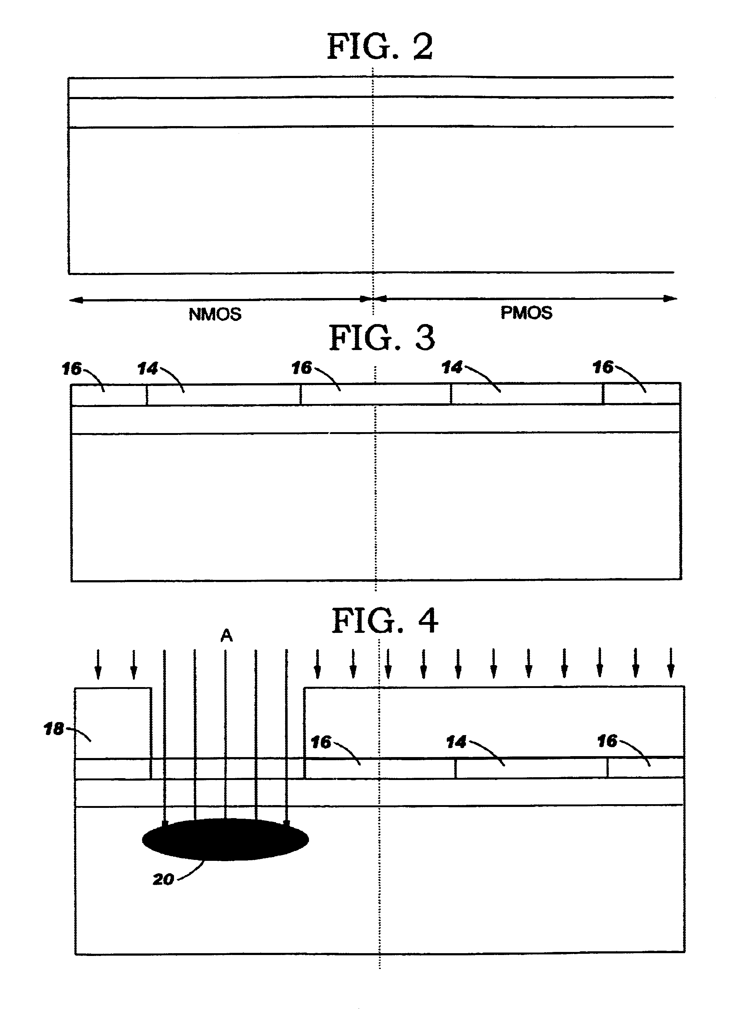
[0013]The invention introduces a method for increasing device performances for both an N type device and a P type device, which is easily integrated into conventional processing steps without significantly increasing manufacturing costs. This is achieved by selectively introducing tensile and compressive strains in portions of a semiconductor substrate or layer on which an N type device and a P type device are formed. In general, the tensile strain is introduced by expanding a portion of the substrate or layer for the N type device, and the compressive strain is introduced by compressing a portion of the substrate or layer for the P type device.

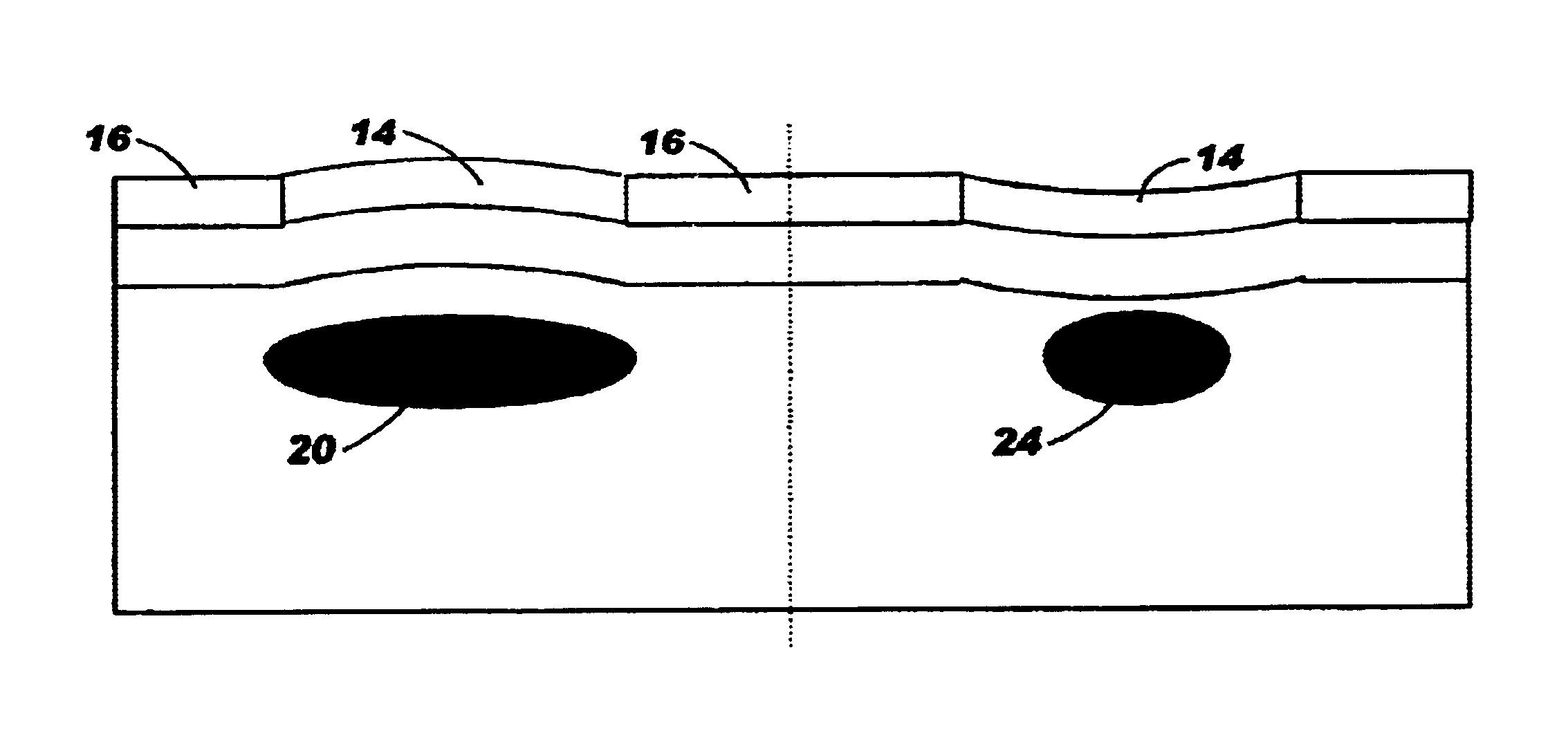
[0014]FIG. 1 illustrates desired stress types for improving the performance of an N type device (e.g., NFET) and a P type device (e.g., PFET). Each of the NFET and PFET has a source region, a gate region and a drain region, as shown therein. The arrows extending outwardly from the active area illustrate tensile stress, and the arrows extendin...


PUM


Abstract

A method for manufacturing a semiconductor device is provided. The method includes forming a semiconductor layer on a substrate. The first region of the substrate is expanded to push up the first portion of the semiconductor layer, thereby applying tensile stress to the first portion. The second region of the substrate is compressed to pull down the second portion of the semiconductor layer, thereby applying compressive stress to the second portion. An N type device is formed over the first portion of the semiconductor layer, and a P type device is formed over the second portion of the semiconductor layer.

Description

BACKGROUND OF INVENTION[0001]The invention generally relates to methods for manufacturing a semiconductor device with improved device performance, and more particularly to methods for manufacturing semiconductor devices by imposing tensile and compressive stresses in the substrate.[0002]Mechanical stresses (e.g., tensile stress and compressive stress) within a semiconductor substrate can modulate device performance, which means stresses within a semiconductor substrate enhance semiconductor device characteristics. Thus, the characteristics of a semiconductor device can be improved by creating tensile and / or compressive stresses in the channel regions of an N type device (e.g., NFET) and / or a P type device (e.g., PFET). However, the same stress component, either tensile or compressive stress, discriminatively affects the characteristics of an N type device and a P type device. For example, when tensile stress is applied to a device in the direction of current flow, the performance of...

Claims


Application Information

Patent Timeline
Patent Type & Authority Patents(United States)
IPC IPC(8): H01L21/762H01L21/70H01L27/12H01L21/84
CPCH01L21/7624H01L27/1203H01L21/84H01L29/7849
Inventor CHIDAMBARRAO, DURESETIDOKUMACI, OMER H.
Owner GLOBALFOUNDRIES INC
Why Eureka
Try Eureka