Design concept for SRAM read margin

a design concept and read margin technology, applied in the field of memory devices, can solve the problems of soft errors, soft errors, adverse effects of sram cell operation, etc., and achieve the effect of improving the read margin of a sram devi

Inactive Publication Date: 2005-05-10
TAIWAN SEMICON MFG CO LTD
View PDF6 Cites 34 Cited by
  • Summary
  • Abstract
  • Description
  • Claims
  • Application Information

AI Technical Summary

Benefits of technology

[0010]A principal object of the present invention is to provide an effective and very manufacturable method to improve the read margin of a SRAM device.

Problems solved by technology

However, as the power supply voltage, VCC, is reduced to below about 1.2 Volts, SRAM cell operation can be adversely affected.
In particular, a very low VCC level can cause soft errors.
Soft errors occur due to the small VCC level reducing the cell reading margin.
In a soft error, a SRAM cell that has correctly maintained the cell state will, nevertheless, be incorrectly read by the sensing circuit due to random effects, such as noise, that cannot be overcome due to insufficient margin.

Method used


Image

  • Design concept for SRAM read margin
  • Design concept for SRAM read margin
  • Design concept for SRAM read margin

Examples


Embodiment Construction

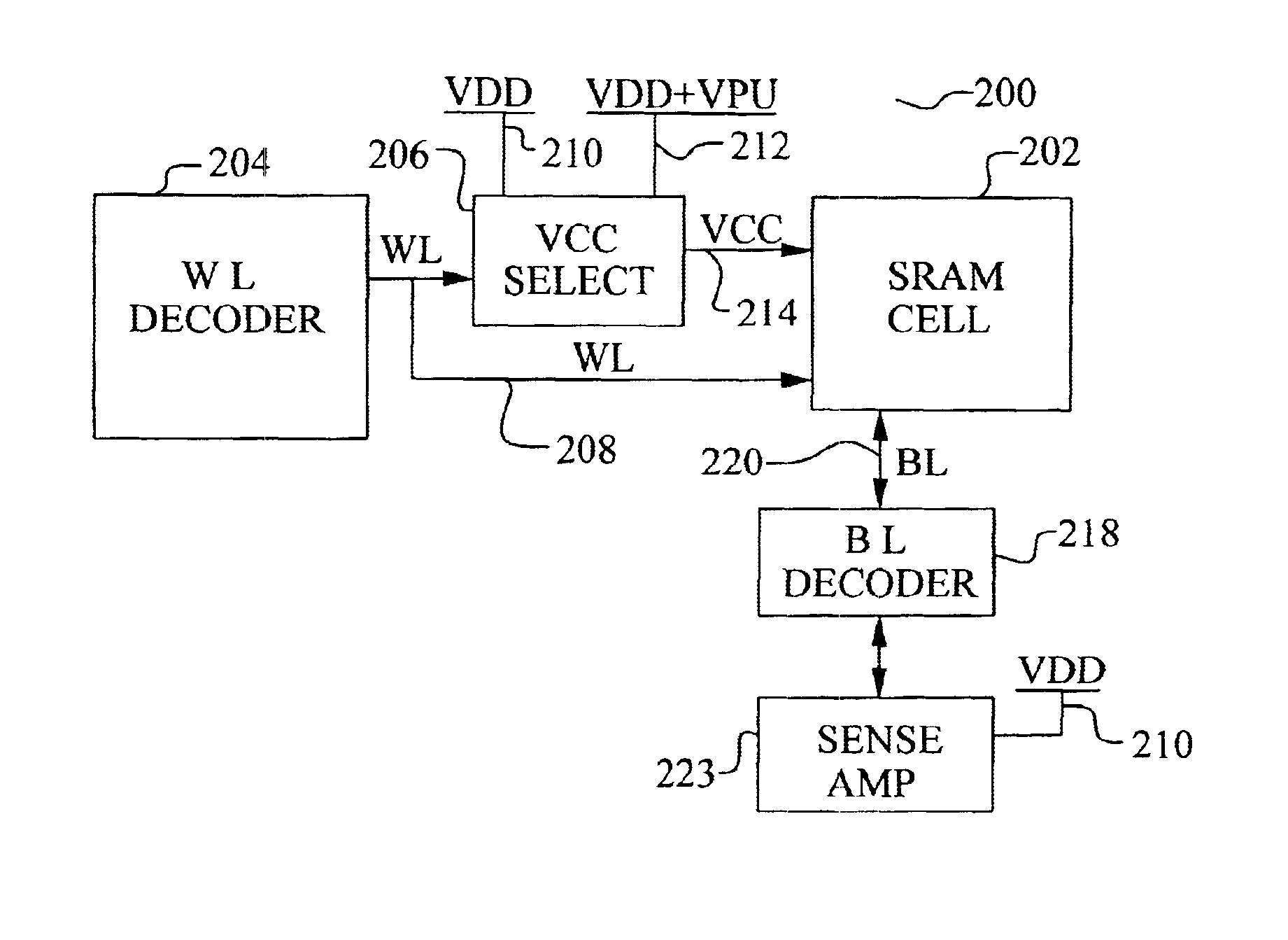
[0024]The preferred embodiments of the present invention disclose a method to improve the reading margin in a SRAM memory device. The method provides a means to control the power supply voltage such that the power supply voltage on cells selected for a reading access can be made larger than the power supply voltage on non-selected cells. It should be clear to those experienced in the art that the present invention can be applied and extended without deviating from the scope of the present invention.

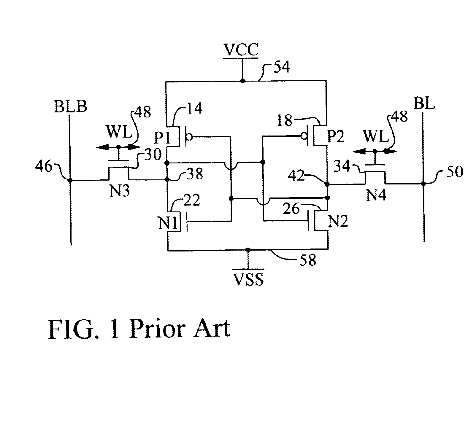
[0025]Referring now to FIG. 4, the preferred embodiment of the present invention is illustrated. Several important features of the present invention are shown and discussed below. The basic concept 200 of the invention is shown. A single SRAM cell 202 is depicted. This SRAM cell 202 may comprise any type of cell architecture known in the art such as 4T or 6T. More preferably, the SRAM cell 202 comprises a 6T architecture as shown in FIG. 1. Referring again to FIG. 4, the SRAM cell 202 is ...


PUM


Abstract

A new method to improve the reading margin in a SRAM memory array is achieved. The method comprises providing an array of SRAM cells. Each SRAM cell has a power supply terminal. A first voltage is forced on the power supply terminal of a first SRAM cell that is selected for reading. A second voltage is forced on the power supply terminal of a second SRAM cell that is not selected for reading. The first voltage does not equal the second voltage. A new SRAM device featuring this method is disclosed.

Description

BACKGROUND OF THE INVENTION[0001](1) Field of the Invention[0002]The invention relates to a memory device, and, more particularly, to a method to improve the reading margin in a SRAM device.[0003](2) Description of the Prior Art[0004]Static memory devices (SRAM) are used in a wide variety of electronics applications. SRAM devices provide a randomly accessible memory array where the data contents can be written and re-written at any time. Further, the SRAM storage cells are constructed such that the static operating current is very low.[0005]Referring now to FIG. 1, an exemplary SRAM memory cell 10 is shown in circuit schematic form. A typical SRAM cell 10 comprises six transistors (6T). A cross-coupled inverter pair N122, P114, N226, and P218 and access transistors N330 and N434 make up the cell 10. The cell is powered by a supply VCC 54. During a write operation, a write data state is set by forcing complimentary voltages (0 and 1) on the bit line (BL) 50 and bit line bar (BLB) 46 ...

Claims


Application Information

Patent Timeline
Patent Type & Authority Patents(United States)
IPC IPC(8): G11C11/419
CPCG11C11/419
Inventor LIAW, JHON-JHY
Owner TAIWAN SEMICON MFG CO LTD
Why Eureka
Try Eureka