Systems and methods for detecting defects in printed solder paste

a technology of printed solder paste and defect detection, applied in the field of machine vision systems, can solve the problems of not having the necessary mass or geometry to adversely affect a given process, gap defects that are actually significant to a process may not always connect adjacent pads, and can not guarantee the existence of bridge-related defects, etc., to achieve the effect of improving the detection of solder paste defects and improving the control of the print process

Inactive Publication Date: 2005-05-10
KPS SPECIAL SITUATIONS FUND II LP
View PDF14 Cites 83 Cited by
  • Summary
  • Abstract
  • Description
  • Claims
  • Application Information

AI Technical Summary

Benefits of technology

[0007]In at least one embodiment, the invention provides systems and methods that can provide improved detection of solder paste defects such as bridges, to improve print process control. In this embodiment, the systems and methods of the invention operate on a premise that not all bridge or “bridge-like” defects have the necessary mass or geometry to adversely affect a given process, and gap defects that are significant don't always connect adjacent pads to form a bridge. Although subsequent processes also play a part in determining the quality of the final assembly, detection and accurate assessment of bridge and ot

Problems solved by technology

The existence of solder paste spanning a gap between adjacent pads, by itself, does not guarantee that a bridge-related defect will occur later in the assembly process.
Not all bridges or bridge-like defects

Method used


Image

  • Systems and methods for detecting defects in printed solder paste
  • Systems and methods for detecting defects in printed solder paste
  • Systems and methods for detecting defects in printed solder paste

Examples


Embodiment Construction

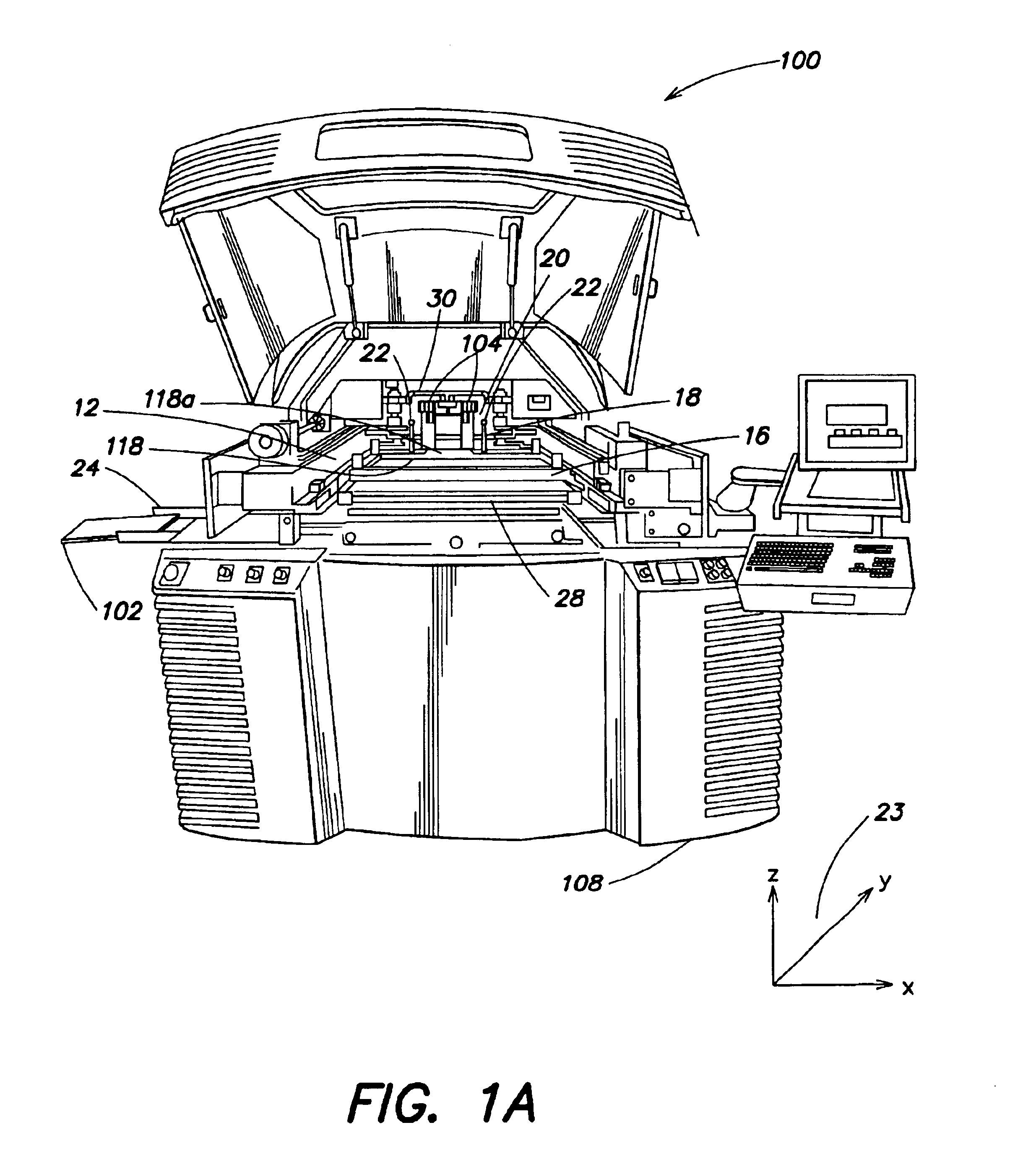
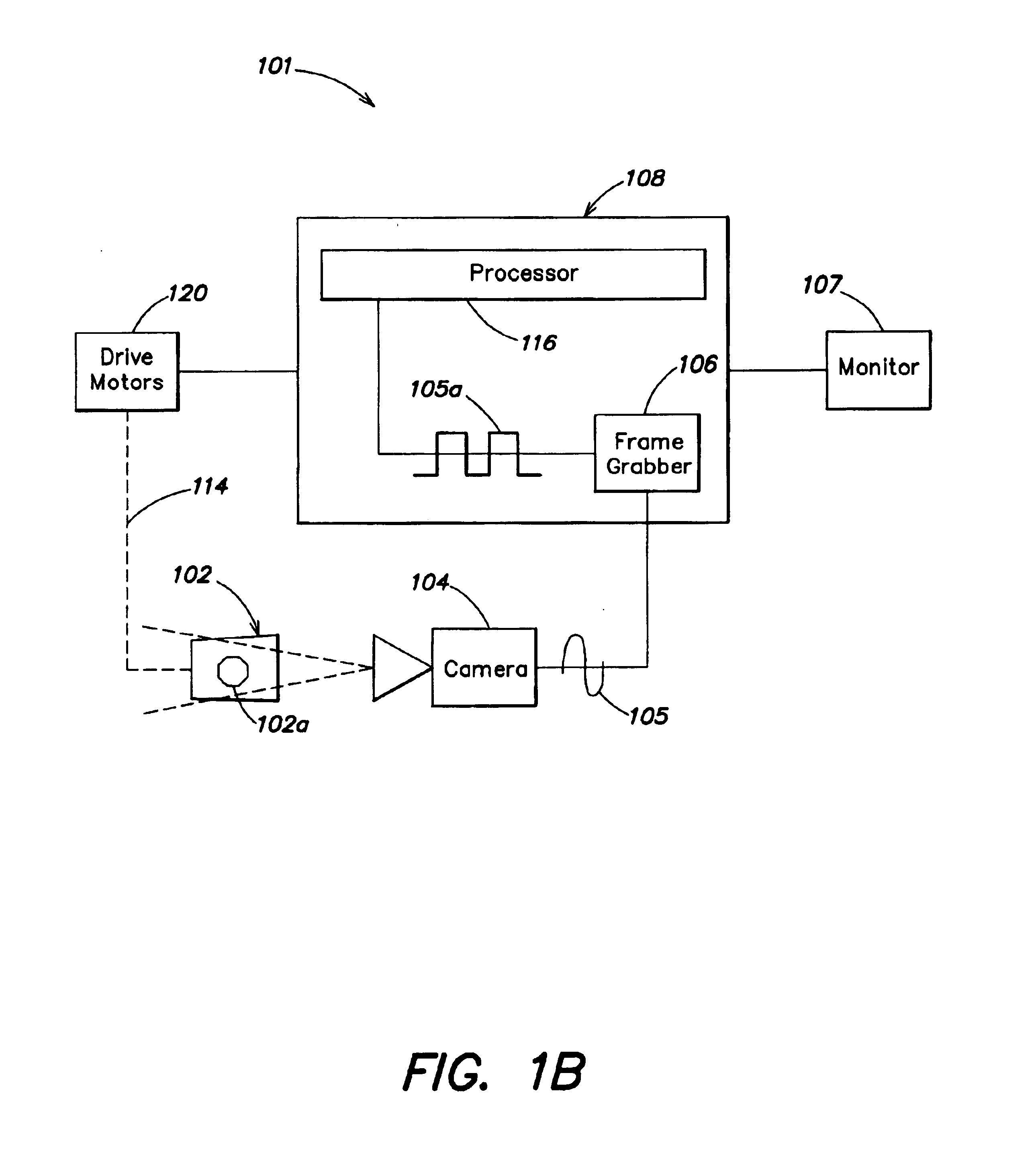
[0053]One embodiment of the present invention generally relates to a stencil printer utilizing a method for conducting solder paste texture recognition. This technique is used to acquire paste-only images of printed substrates, such as stencils and circuit boards, for use in analyzing and thereafter preventing defects. For example, print defects often occur in the process of printing solder paste on a circuit board using a stencil printer. FIG. 1A shows a front view of a stencil printer 100 in accordance with one embodiment of the present invention. The stencil printer 100 includes a frame 12 that supports components of the stencil printer including a controller 108, a stencil 16, and a dispensing head 118 having a dispensing slot 118a from which solder paste may be dispensed.

[0054]The dispensing head 118 is coupled to a first plate 18 using two thumbscrews 22. The first plate 18 is coupled to a second plate 20 which is coupled to the frame 12 of the stencil printer 10. The first pl...


PUM

PropertyMeasurementUnit
Grain sizeaaaaaaaaaa

Abstract

A method of analyzing an image of a substance deposited onto a substrate, the image comprising a plurality of pixels, includes defining a region of interest in the image, associating the region of interest with first and second perpendicular axis, wherein a set of pixels in the image lie along the first axis, converting the pixels in the region of interest to a single dimensional array aligned with the first axis and projecting along the second axis, and applying at least one threshold to the single dimensional array, the threshold based at least in part on a predetermined limit.

Description

CLAIM OF PRIORITY[0001]This application is a continuation-in-part of U.S. patent application Ser. No. 09 / 304,699 filed May 4, 1999 now U.S. Pat. No. 6,738,505, entitled “A method and apparatus for inspecting solder paste deposits on substrates”, the contents of which are incorporated herein by reference in their entirety.FIELD OF THE INVENTION[0002]Embodiments of the invention generally relate to devices, systems, and methods used in machine vision systems. More particularly, the invention relates to systems and methods for detecting defects in the solder paste print process.BACKGROUND OF THE INVENTION[0003]In typical surface-mount circuit board manufacturing operations, a stencil printer is used to print solder paste onto a circuit board. Typically, a circuit board having a pattern of pads or some other, usually conductive, surface onto which solder paste will be deposited is automatically fed into the stencil printer and one or more small holes or marks on the circuit board, calle...

Claims


Application Information

Patent Timeline
IPC IPC(8): B23K3/08B23K3/00G01N21/956G01N21/88H05K3/34H05K3/12H05K1/02B23K1/00G01B11/00B23K31/12G06K9/00G06TG06T1/00G06T7/00G06T7/40G06T9/00
CPCB23K1/0016B23K31/12G01N21/95607G01N21/95684G06T7/0004G06T7/403H05K3/3484B23K3/08H05K2203/0126B23K2201/40B23K2201/42G01N2021/95646G01N2021/95669G06T2207/30152H05K1/0269H05K3/1216G06T7/44B23K2101/40B23K2101/42H05K3/3485G06T9/00
Inventor PRINCE, DAVID P.
Owner KPS SPECIAL SITUATIONS FUND II LP
Why Eureka
Try Eureka