Liquid crystal device and manufacturing method thereof

a technology of liquid crystal devices and manufacturing methods, applied in non-linear optics, instruments, optics, etc., can solve the problems of reducing the strength of substrates to make them easy to break, generating cracks on substrates, and difficult to uniformly support a wide area of terraces, etc., to enhance the protective property of wiring lines

Inactive Publication Date: 2005-05-17
138 EAST LCD ADVANCEMENTS LTD
View PDF24 Cites 27 Cited by
  • Summary
  • Abstract
  • Description
  • Claims
  • Application Information

AI Technical Summary

Benefits of technology

[0012]According to the liquid crystal device of the first embodiment of the present invention, a resin molding step may be eliminated besides enabling the wiring lines to be securely protected from electrolytic corrosion without requiring additional manufacturing steps, by forming an insulation film on the liquid crystal seal area as well as on the surface of the terrace area so as to cover the wiring lines. In addition, since the surface of the terrace area can be flattened, the surface of the terrace area

Problems solved by technology

However, thinning the transparent substrates 11 and 12 results in decreased strength of the substrates to make them to be easily broken, while arising a possibility that cracks are generated on the substrate particularly at the terrace area 11a where only the transpa

Method used


Image

  • Liquid crystal device and manufacturing method thereof
  • Liquid crystal device and manufacturing method thereof
  • Liquid crystal device and manufacturing method thereof

Examples


first embodiment

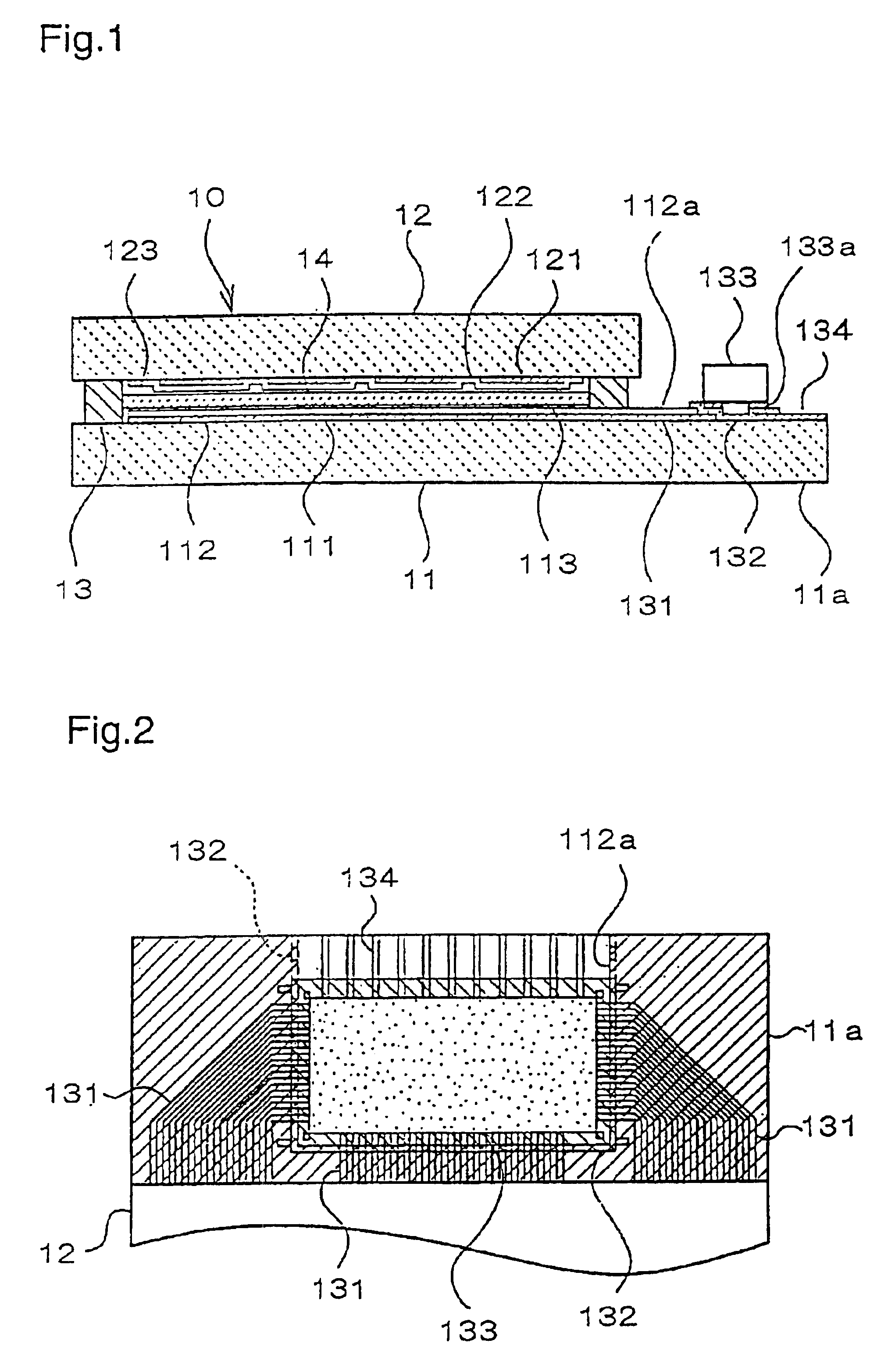
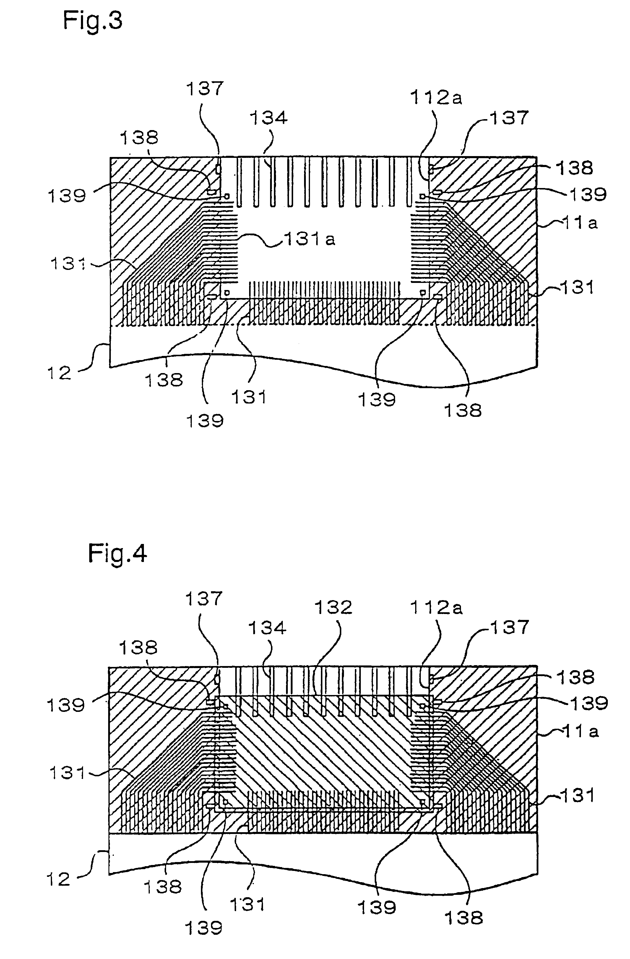
[0102]The insulation film 112 formed within the liquid crystal seal area is extended onto the terrace area 11a in the In other words, the insulation film 112 formed within the liquid crystal seal area is continuous to the extended formation portion 112a in order to enhance protected state with the insulation film, such as prevention of electrolytic corrosion of the wiring lines. However, the insulation film 112 may be formed into mutually isolated two portions of the insulation film formed within the liquid crystal seal area, and the extended formation portion 112a on the surface of the terrace area 11a in the present invention.

[0103]While the insulation film 112 as an overcoat layer is formed on the surface of the terrace area 11a in order to prevent short circuit of the liquid crystal device in the foregoing first embodiment, forming an insulation film other than the overcoat layer on the surface of the terrace area 11a is effective as well. Otherwise, the orientation film 113 ma...

second embodiment

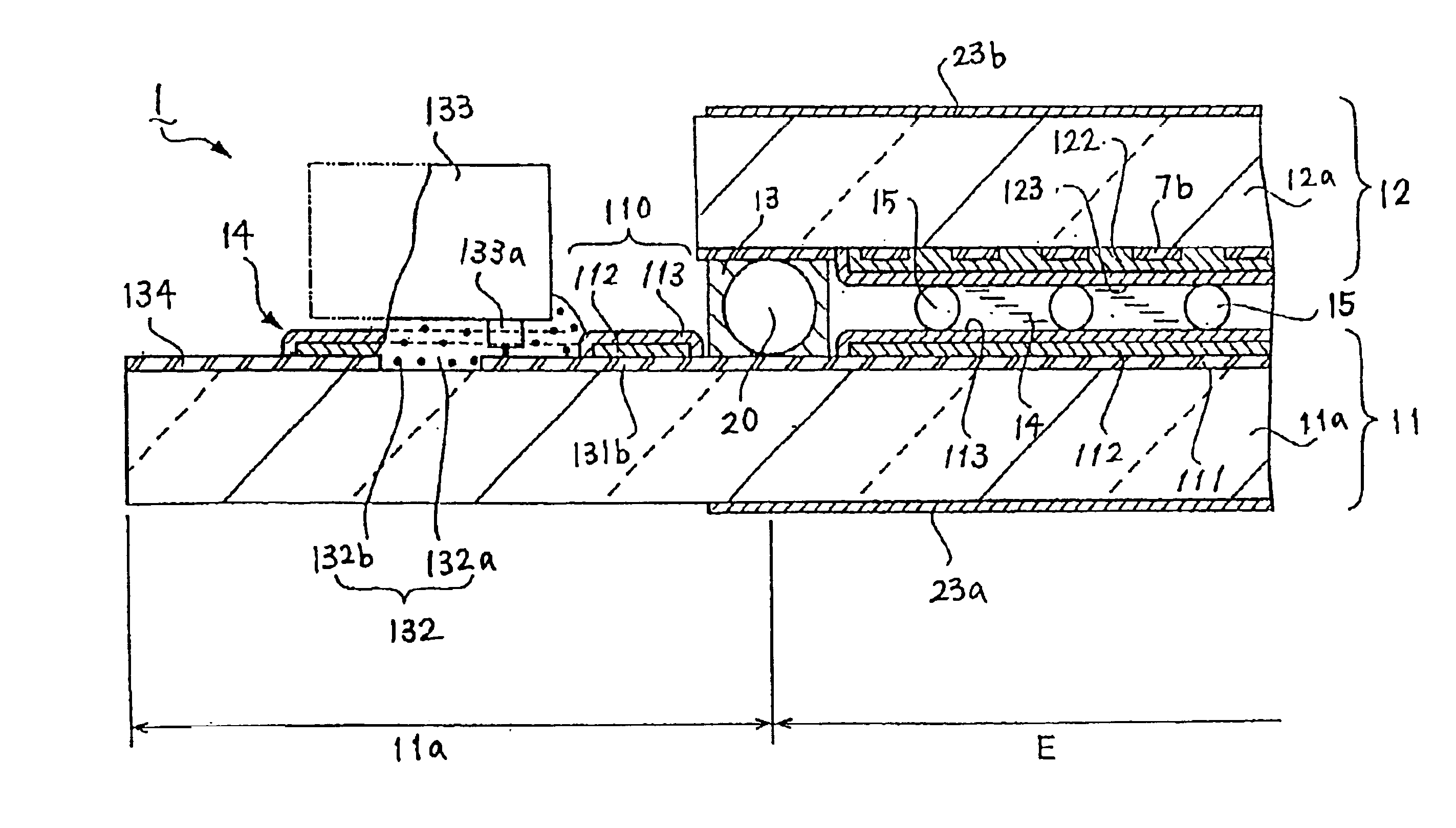
[0106]FIGS. 7 and 8 show the liquid crystal device according to the present invention. This liquid crystal device 1 comprises a pair of substrates 11 and 12, and the circumferences of them are bonded to one another with a seal member 13. These substrates 11 and 12 are constructed by mounting various elements on virgin substrates 11a and 12a made of a glass or a flexible material such as a plastic.

[0107]The dimension of a gap formed between these substrates 11 and 12, so called a cell gap, is determined to be uniform, for example about 5 μm, with a plurality of spacers 15, and a liquid crystal 14 is sealed within the cell gap surrounded by the seal member 13. The member denoted by the reference numeral 13a in FIG. 7 is a liquid crystal injection port formed at a part of the seal member 13. The liquid crystal 14 is injected into the cell gap through the liquid crystal injection port13a, which is sealed with a resin after completing injection of the liquid crystal.

[0108]First electrode...

third embodiment

[0136]FIGS. 14 and 15 show the third embodiment according to the present invention. This liquid crystal device 1 comprises a pair of substrates 11 and 12 in which their circumferences are bonded to one another with a seal member 13. This seal member 13 is formed by, for example, printing. These substrates 11 and 12 are manufactured by forming various elements on virgin substrates 11a and 12a made of a rigid material such as a glass, or a flexible film such as a plastic.

[0137]The gap formed between these substrates 11 and 12, or the so-called cell gap, is controlled to have a uniform width of, for example, about 5 μm with a plurality of spacers 15, and a liquid crystal 14 is sealed within an area surrounded by the seal member 13 in the cell-gap. The reference numeral 13a in FIG. 14 denotes a liquid crystal injection port formed at a part of the seal member 13. The liquid crystal 14 is injected into the cell-gap through the liquid crystal injection port 13a, and the liquid crystal inj...


PUM


Abstract

For providing a liquid crystal device comprising a structure capable of uniformly supporting a terrace area in the liquid crystal device, a pair of insulation films 112 are formed on the terrace area 11a so as to cover a part of wiring lines 131a and 131b simultaneously with forming the insulation films 112 on electrodes 111 using the same material as the insulation film on the electrodes, and an orientation film 113 is additionally formed on the insulation films 112. The orientation film 113 is also formed on the insulation films 112 formed on the terrace area 11a, and the orientation film 113 is formed so as to expand out of the outer edge of the insulation films 112.

Description

TECHNICAL FIELD[0001]The present invention relates to a liquid crystal device and a manufacturing method thereof. The present invention particularly relates to a structure of a terrace area comprising wiring lines pulled out of a liquid crystal seal area.BACKGROUND ART[0002]Conventional liquid crystal devices are constructed by bonding a pair of transparent substrates to one another via a seal member, and sealing a liquid crystal between the substrates inside of the seal member, or within a liquid crystal seal area.[0003]One example of the structure of the liquid crystal devices is shown in FIGS. 31(a) and 31(b). FIG. 31(a) is a planar perspective view illustrating the planar structure of the liquid crystal device 1, and FIG. 31(b) is an enlarged cross section illustrating the structure in the vicinity of a terrace area 11a in the liquid crystal device 1. The liquid crystal device 1 comprises two sheet of transparent substrates 11 and 12 bonded to one another via a seal member 13. T...

Claims


Application Information

Patent Timeline
IPC IPC(8): G02F1/13G02F1/1333G02F1/1337G02F1/1345
CPCG02F1/133345G02F1/13452G02F2001/13456G02F1/1337G02F1/13456G02F1/1345
Inventor HAGIWARA, TAKESHISUEHIRO, KEIICHISHIMIZU, TETSUO
Owner 138 EAST LCD ADVANCEMENTS LTD
Why Eureka
Try Eureka