
Liquid crystal display device and electronic apparatus comprising it

a technology of liquid crystal display device and electronic device, which is applied in the direction of semiconductor devices, optics, instruments, etc., can solve the problems of obstructing the reduction of the thickness of the mobile phone itself, affecting the compactness, and increasing the thickness of the device using the liquid crystal display device as a display unit. achieve the effect of smaller area and greater thinness

Inactive Publication Date: 2005-05-24
SONY CORP
View PDF7 Cites 29 Cited by
  • Summary
  • Abstract
  • Description
  • Claims
  • Application Information

AI Technical Summary

Benefits of technology

[0011]An object of the present invention is to provide a liquid crystal display device enabling the realization of a greater thinness, smaller area, and narrower frame of the liquid crystal display device.
[0012]Another object of the present invention is to provide an electronic device enabling the realization of a greater thinness, smaller area, and narrower frame overall by mounting such a liquid crystal display device.

Problems solved by technology

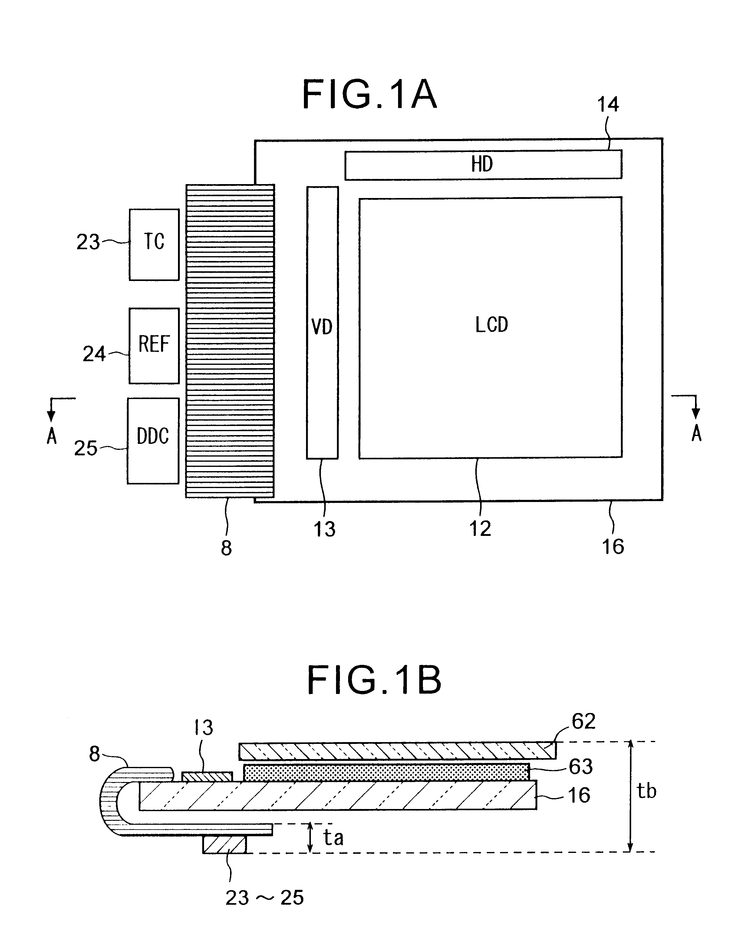
Therefore, the thickness of the device using the liquid crystal display device as a display unit also ends up becoming greater.
If the thickness tb of the liquid crystal display device used as the display unit of a mobile phone is great, this would obstruct the reduction of thickness of the mobile phone itself.
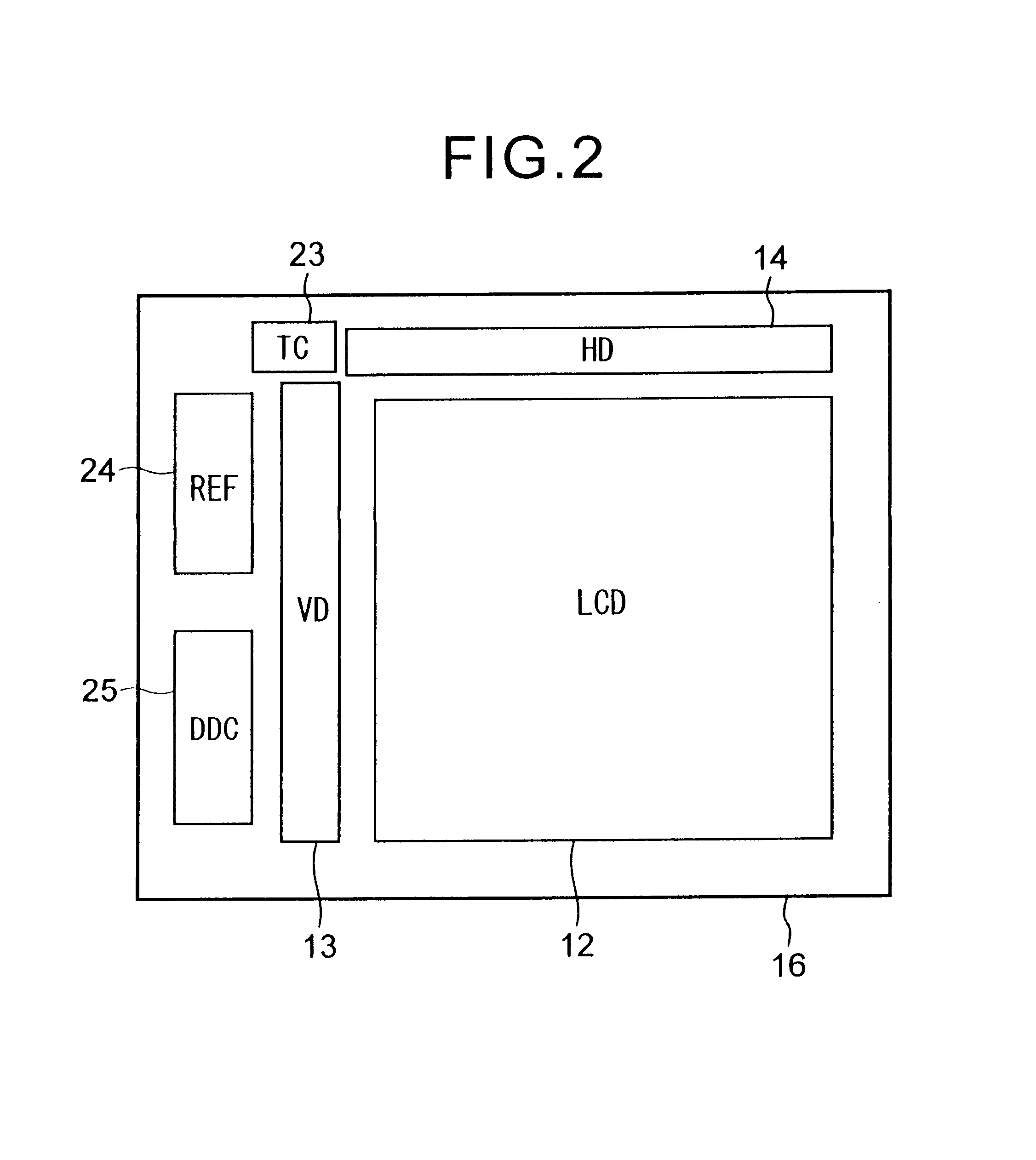
Further, in the liquid crystal display device shown in FIG. 2, the total area of the peripheral circuits formed by the TFTs and the remaining IC chips 23 to 25 becomes the area of the periphery (frame), so there is the disadvantage that compactness is impaired.
Further, there is the disadvantage that the ratio of the effective display area (liquid crystal display unit) in the liquid crystal display device ends up becoming smaller.

Method used


Image

  • Liquid crystal display device and electronic apparatus comprising it
  • Liquid crystal display device and electronic apparatus comprising it
  • Liquid crystal display device and electronic apparatus comprising it

Examples


first embodiment

[0029

[0030]The present embodiment shows the application of the present invention to an active matrix type liquid crystal display device of an analog dot sequential driving system.

[0031]FIG. 3A is a schematic view of the configuration of the circuits of a liquid crystal display device according to the present embodiment, while FIG. 3B is a sectional view along the line B—B in FIG. 3A.

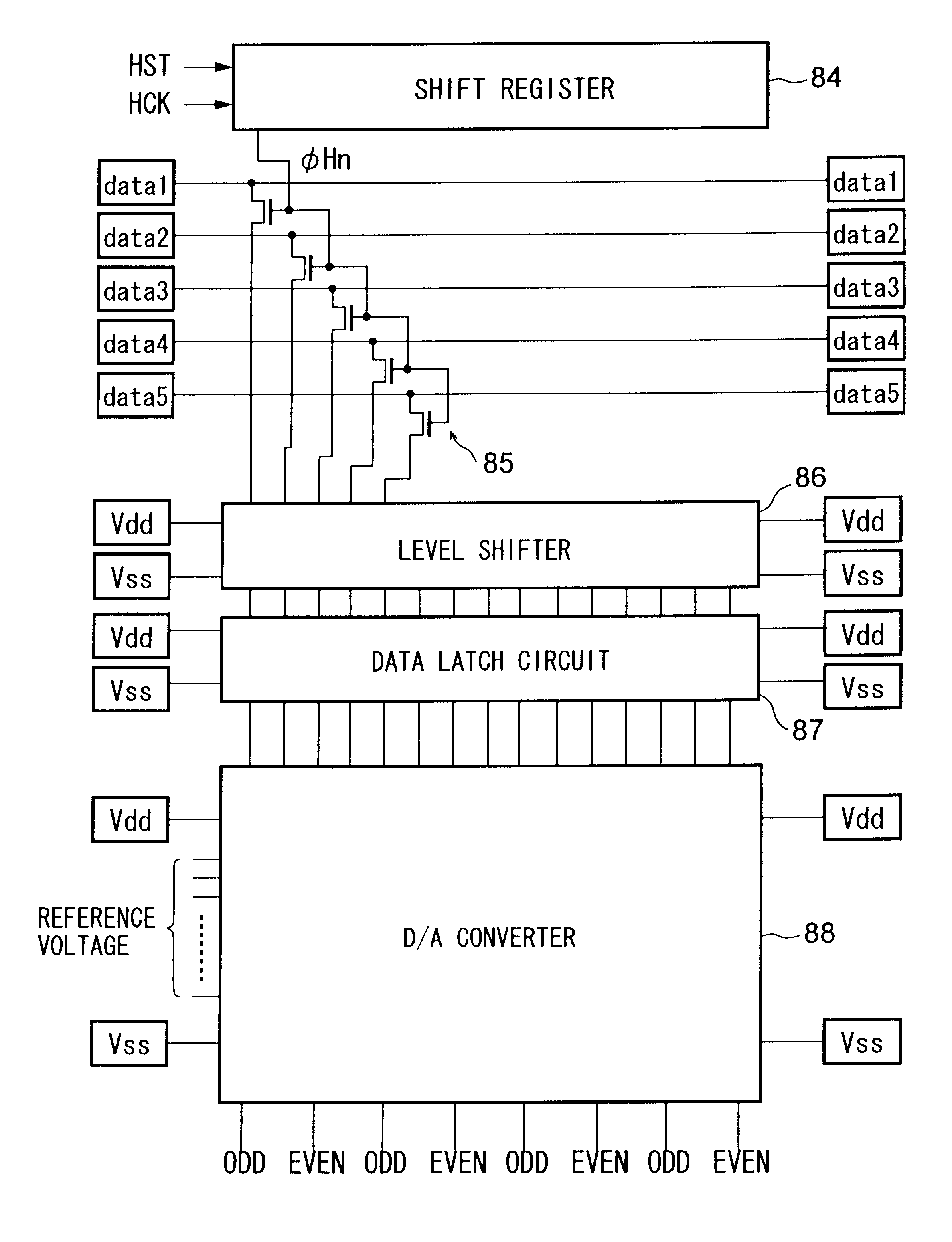
[0032]Further, FIG. 4 is a schematic view of the electrical connections of the circuits forming the liquid crystal display device according to the present embodiment.

[0033]As shown in FIG. 3A and FIG. 4, the active matrix type liquid crystal display device according to the present embodiment has a liquid crystal display unit 12 comprised of a large number of pixels 11 arranged in a matrix, a vertical driver (VD) 13 for sequentially selecting the pixels 11 of the liquid crystal display unit 12 in row units, a horizontal driver (HD) 14 for writing pixel signals into the pixels 11 selected in row units, and...

second embodiment

[0085

[0086]The present embodiment shows application of the present invention to an active matrix type liquid crystal display device of a time-division driving system (selector system).

[0087]FIG. 9 is a schematic view of the layout of the circuits of an active matrix type liquid crystal display device of the time-division driving system to which the present invention is applied.

[0088]FIG. 10 is a schematic view of electrical connections of circuits of the liquid crystal display device shown in FIG. 9.

[0089]In FIG. 9 and FIG. 10, the liquid crystal display device according to the present embodiment is comprised of a liquid crystal display unit 12 comprised of a large number of pixels 11 arranged in a matrix, a vertical driver (VD) 13 for sequentially selecting the pixels 11 of the liquid crystal display unit 12 in row units, a horizontal driver (HD) 74 for writing pixel signals into the pixels 11 selected in row units, a time-division switch unit (SW) 75 for time-division driving, and...

third embodiment

[0124

[0125]The liquid crystal display devices according to the above first and second embodiments are suitable not only for use as display units of personal computers, word processors, and other office automation equipment or television receivers etc., but also particularly for use as display units of portable electronic devices such as mobile phones and PDAs (personal digital assistants), which are being made thinner and thinner.

[0126]FIG. 13 is a perspective view of the schematic configuration of for example a PDA as an electronic device mounting a liquid crystal display device according to the first and second embodiments.

[0127]The PDA according to this example is configured with a display unit 92, a speaker unit 93, an operation unit 94, and a power source unit 95 arranged at the front surface of the device housing 91.

[0128]Note that input to the PDA shown in FIG. 13 is possible by a pen 96 etc. on the display unit 92.

[0129]While not shown, the device housing 91 houses inside it...


PUM

PropertyMeasurementUnit
thickness taaaaaaaaaaa
compositionaaaaaaaaaa
voltageaaaaaaaaaa

Abstract

A liquid crystal display device enabling realization of greater thinness, smaller area, and narrower frame and an electronic device using the same are provided. For this purpose, the liquid crystal display device of the present invention comprises a first substrate, a pixel unit formed on the first substrate and having pixels arranged in a matrix, a second substrate arranged facing the first substrate, a liquid crystal composition held between the first substrate and the second substrate, and peripheral circuits formed on the first substrate for writing pixel signals to the pixel unit, at least part of the peripheral circuits of the above peripheral circuits being formed by thin film transistors on the first substrate, the remaining part of the peripheral circuits of the above peripheral circuits being formed by semiconductor chips, and the semiconductor chips being arranged on the first substrate so that at least part of the semiconductor chips overlap the regions of the peripheral circuits formed by the thin film transistors.

Description

TECHNICAL FIELD[0001]The present invention relates to a liquid crystal display device and an electronic device using the same, more particularly relates to a liquid crystal display device used for a portable electronic device where greater thinness, smaller area, and a narrower frame are demanded and to an electronic device using the same as a display unit.BACKGROUND ART[0002]Thin, low power consuming panel displays have come to be used in large numbers as display devices for television receivers, computers, and portable terminals in recent years.[0003]As such a panel display, there is known an active matrix type display device comprised of a large number of pixels using for example TFTs (thin film transistors) as switching elements arranged in a matrix on a glass substrate or other transparent insulating substrate (panel) in combination with liquid crystals or other substances having an electro-optic effect.[0004]As such an active matrix type display device, Japanese Unexamined Pat...

Claims


Application Information

Patent Timeline
Patent Type & Authority Patents(United States)
IPC IPC(8): G02F1/13G02F1/1362G02F1/1345G02F1/133
CPCG02F1/13454G02F1/13452H01L2224/16225G02F1/1345
Inventor INO, MASUMITSU
Owner SONY CORP
Learn More