Flash memory with protruded floating gate

a floating gate and flash memory technology, applied in the field of flash memory, can solve the problems of reducing the surface area of floating gates, limiting the miniaturization of memory cells, and the difficulty of shrinking the cell size in the fabrication of nonvolatile memory cells, so as to reduce the capacitance cfs, increase the coupling ratio, and reduce the size

Inactive Publication Date: 2005-06-21
VANGUARD INTERNATIONAL SEMICONDUCTOR CORPORATION
View PDF3 Cites 2 Cited by
  • Summary
  • Abstract
  • Description
  • Claims
  • Application Information

AI Technical Summary

Benefits of technology

[0013]In the present invention, a nonvolatile semiconductor memory device with an increased coupling ratio is disclosed. This is accomplished by providing a reduced size floating gate which reduces the capacitance Cfs between the floating gate and the semiconductor substrate. The effect is the same as increasing the capacitance Ccf between the control gate and the floating gate.
[0014]Accordingly, the object of the present invention is to provide a flash memory with protruded floating gate and method for forming the same. This invention provides a novel way of erasing, and increases the access rate by improving the capacitive coupling ratio of the flash memory by increasing the surface area.

Problems solved by technology

However, it is very difficult to shrink the cell size in the fabrication of nonvolatile memory cells when the conventional local oxidation (LOCOS) isolation technique is used.
The isolation structure formed by this technique has a very large dimension and thus limits the miniaturization of the memory cells.
However, as component dimensions continue to shrink, the surface area of floating gates also shrinks.
This leads directly to a decrease in capacitance of the effective capacitor formed between the floating gate layer and the control gate layer.
The poorly-coupled voltage to floating gate limits the programming and accessing speed characteristics of the memory device.

Method used


Image

  • Flash memory with protruded floating gate
  • Flash memory with protruded floating gate
  • Flash memory with protruded floating gate

Examples


Embodiment Construction

[0023]A detail description of the method of forming the flash memory with protruded floating gate of the present invention is given hereafter with reference to FIGS. 2a to 2b.

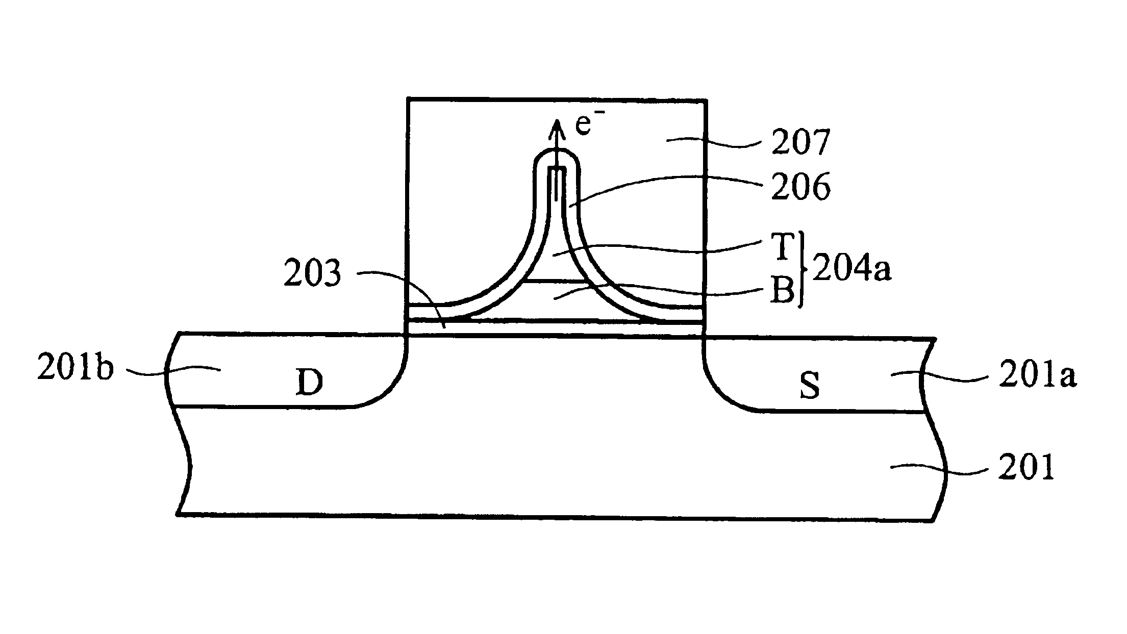
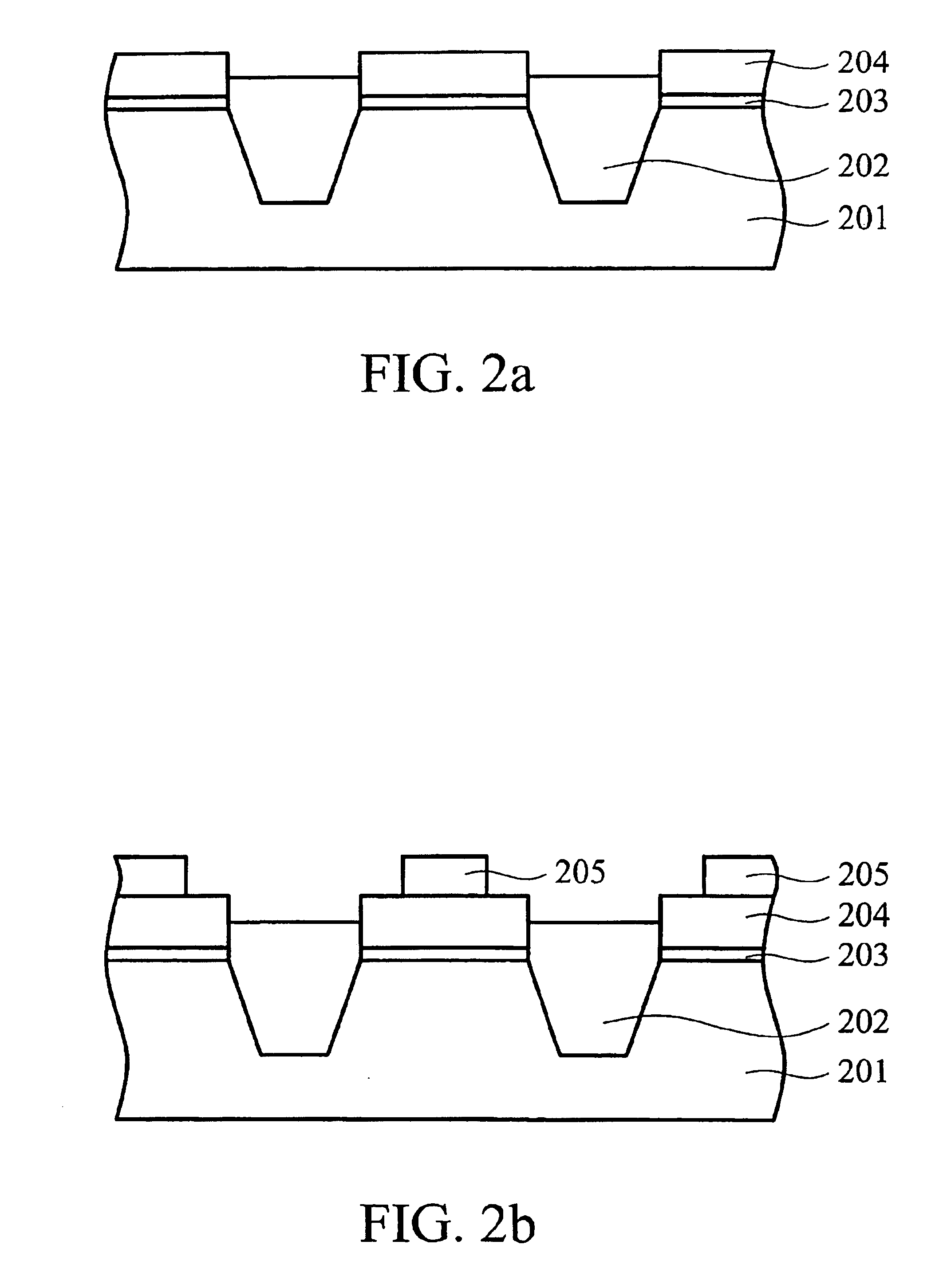
[0024]In FIG. 2a, a substrate 201 is provided. The substrate 201 has an isolation area 202. A plurality of gate oxide 203 is formed on the substrate 201. A plurality of patterned conductive layers 204 is formed on the gate oxide 203, and the isolation area 202 protrudes from the upper surface of the substrate 201 to isolate the patterned conductive layers 204. The isolation area 202 may be a Shallow Trench Isolation (STI).

[0025]With reference to FIG. 2b, the photo resist 205 is formed on the patterned conductive layers 204 after the patterned conductive layers 204 are formed on the substrate 201. The surface area of the photo resist layer 205 is smaller than those of the patterned conductive layers 204.

[0026]As shown in FIG. 2c, the patterned conductive layers 204 are isotropicaly etched with etchant using the...


PUM


Abstract

A method of forming a flash memory with a protruded floating gate. A substrate is provided. An isolation area and a plurality of patterned conductive layers are sequentially formed on the substrate. The isolation area protrudes from the upper surface of the substrate to isolate the patterned conductive layers. A photo resist layer is formed on the patterned conductive layer. The present invention also provides a flash memory with a protruded floating gate comprised a substrate, a plurality of protruded floating gates, an insulator, and a control gate.

Description

CROSS REFERENCE TO RELATED APPLICATIONS[0001]This application is a division of 10 / 158,927 filed Jun. 3, 2002.BACKGROUND OF THE INVENTION[0002]1. Field of the Invention[0003]The present invention relates to a flash memory, and more particularly, to a flash memory with a protruded floating gate.[0004]2. Description of the Prior Art[0005]High-density nonvolatile memory devices have been receiving much attention for application in many fields. One of the most important factors is the low cost of the reduced size of each memory cell. However, it is very difficult to shrink the cell size in the fabrication of nonvolatile memory cells when the conventional local oxidation (LOCOS) isolation technique is used. The isolation structure formed by this technique has a very large dimension and thus limits the miniaturization of the memory cells.[0006]Another isolation technique called shallow trench isolation (STI) has been introduced to the fabrication of nonvolatile memory devices to reduce the...

Claims


Application Information

Patent Timeline
Patent Type & Authority Patents(United States)
IPC IPC(8): H01L21/02H01L21/28H01L29/423H01L29/66H01L29/40H01L29/788
CPCH01L21/28273H01L29/7884H01L29/42324H01L29/40114
Inventor HSU, SCOTT
Owner VANGUARD INTERNATIONAL SEMICONDUCTOR CORPORATION
Why Eureka
Try Eureka