Nonvolatile semiconductor memory device and manufacturing method thereof

a semiconductor memory and non-volatile technology, applied in semiconductor devices, solid-state devices, instruments, etc., can solve the problems of reducing device parameters such as the characteristic deterioration of memory transistors, deterioration of tunnel insulating films, and reducing device parameters such as mutual conductance (gm) representing on characteristics, etc., to achieve the effect of reducing writing voltage and erasing voltage, suppressing reading errors, and increasing coupling ratio

Inactive Publication Date: 2009-11-19
SEMICON ENERGY LAB CO LTD
View PDF20 Cites 15 Cited by
  • Summary
  • Abstract
  • Description
  • Claims
  • Application Information

AI Technical Summary

Benefits of technology

[0023]According to one embodiment of the present invention, by providing each of the semiconductor layer for writing operation and erasing operation, and the semiconductor layer for reading operation, even in the case where writing and erasing are repeatedly performed, reading error can be suppressed. In addition, according to one embodiment of the present invention, the semiconductor layer for reading operation function as a control gate when writing operation and erasing operation are performed, so that the coupling ratio is increased, whereby writing voltage and erasing voltage can be reduced while increase in the area of a memory transistor is controlled.

Problems solved by technology

As a result, the tunnel insulating film is deteriorated and characteristic deterioration of the memory transistor is generated by increase of an interface state density between the semiconductor layer and the tunnel insulating film, increase of an interface state density between the tunnel insulating film and the floating gate, charge injection to the tunnel insulating film, generation of traps, and the like.
For example, by performing writing and erasing repeatedly, there is a possibility that a device parameter such as mutual conductance (gm) representing ON characteristics decreases and reading error occurs.

Method used


Image

  • Nonvolatile semiconductor memory device and manufacturing method thereof
  • Nonvolatile semiconductor memory device and manufacturing method thereof
  • Nonvolatile semiconductor memory device and manufacturing method thereof

Examples


embodiment 1

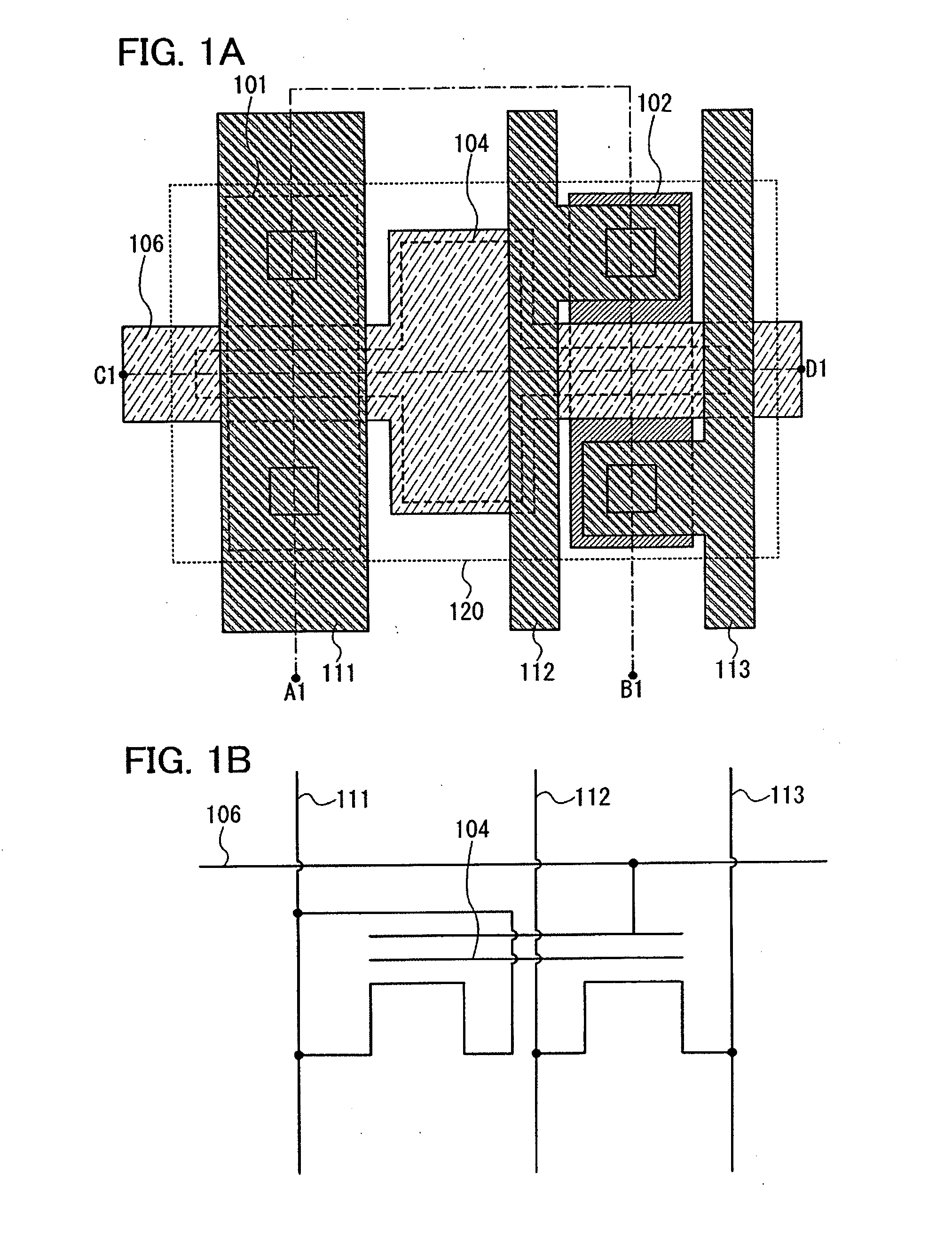
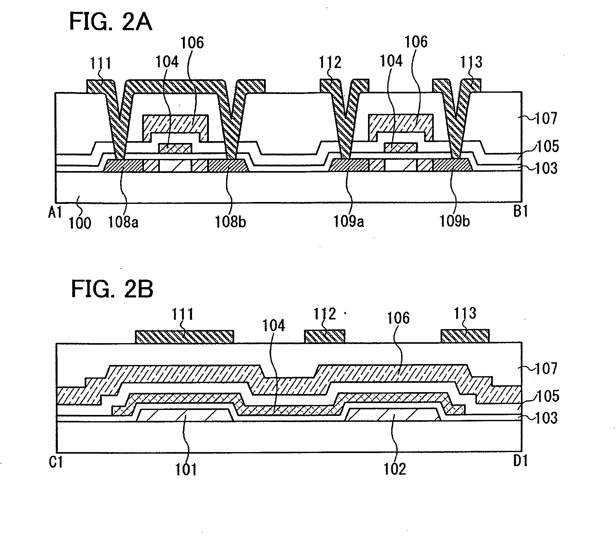
[0036]This embodiment describes an example of a nonvolatile semiconductor memory device with reference to drawings. Note that FIG. 1A illustrates a top view of a memory transistor constituting part of nonvolatile semiconductor memory device, and FIG. 1B illustrates an equivalent circuit diagram of the memory transistor in FIG. 1A. Further, FIG. 2A corresponds to a cross section taken along a line A1-B1 in FIG. 1A, and FIG. 2B corresponds to a cross section taken along a line C1-D1 in FIG. 1A.

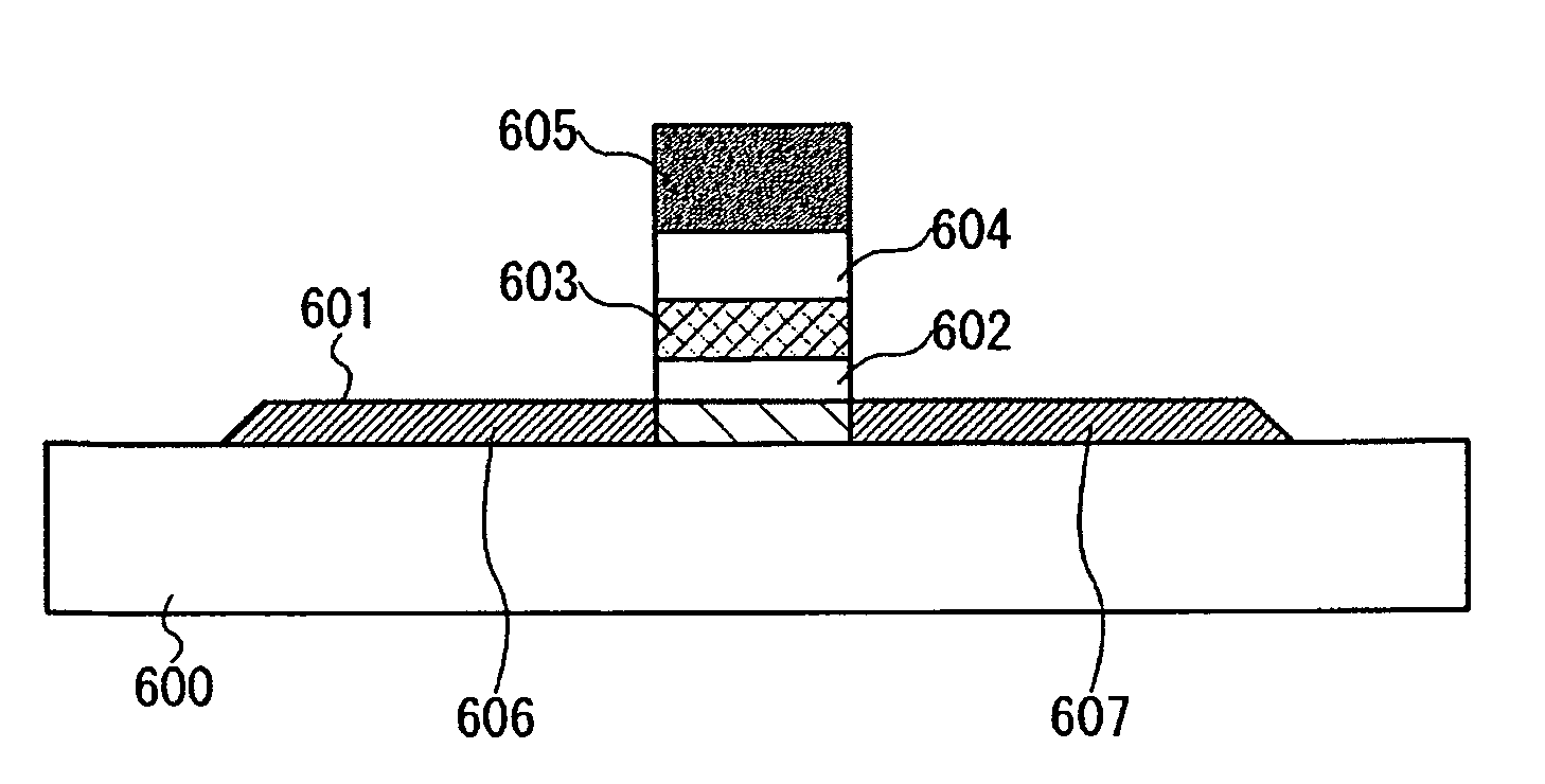
[0037]A nonvolatile semiconductor memory device illustrated in this embodiment includes a memory transistor 120 provided over a substrate 100, which functions as a memory by performing operation of writing, erasing, or reading data on the memory transistor 120.

[0038]The memory transistor 120 includes a first semiconductor layer 101 and a second semiconductor layer 102 provided over a substrate 100, a floating gate 104 provided above the first semiconductor layer 101 and the second semiconductor ...

embodiment 2

[0066]This embodiment describes an example of a method for manufacturing a memory transistor constituting part of the nonvolatile semiconductor memory device described in the above embodiment with reference to drawings. Note that the FIGS. 3A to 3F correspond to a cross section taken along a line A1-B1 in FIG. 1A, and FIGS. 4A to 4D corresponds to a cross section taken along a line C1 to D1 in FIG. 1A.

[0067]First, the first semiconductor layer 101 and the second semiconductor layer 102, each of which has an island shape, are formed over the substrate 100 (see FIGS. 3A and 4A).

[0068]A substrate having an insulating surface, for example, a glass substrate, a quartz substrate, a ceramic substrate, a plastic substrate, or the like can be used as the substrate 100. Further, an insulating film formed of one layer or a plurality of layers may be provided over the surface of the substrate 100 and the first semiconductor layer 101 and the second semiconductor layer 102 may be formed over the...

embodiment 3

[0102]This embodiment describes an application example of a semiconductor device which is provided with the nonvolatile semiconductor memory device described in the above embodiments and in which data can be inputted and outputted without contact, with reference to drawings. The semiconductor device in which data can be inputted and outputted without contact is also called an RFID tag, an ID tag, an IC tag, an IC chip, an RF tag, a wireless tag, an electronic tag, or a wireless chip depending on its usage mode.

[0103]A semiconductor device 800 has a function of communicating data without contact, and includes a high-frequency circuit 810, a power supply circuit 820, a reset circuit 830, a clock generating circuit 840, a data demodulating circuit 850, a data modulating circuit 860, a controlling circuit 870 which controls another circuit, a memory circuit 880, and an antenna 890 (FIG. 8A). The high-frequency circuit 810 receives a signal from the antenna 890 and outputs a signal which...


PUM


Abstract

An object is to suppress reading error even in the case where writing and erasing are repeatedly performed. Further, another object is to reduce writing voltage and erasing voltage while increase in the area of a memory transistor is suppressed. A floating gate and a control gate are provided with an insulating film interposed therebetween over a first semiconductor layer for writing operation and erasing operation and a second semiconductor layer for reading operation which are provided over a substrate; injection and release of electrons to and from the floating gate are performed using the first semiconductor layer; and reading is performed using the second semiconductor layer.

Description

TECHNICAL FIELD[0001]The present invention relates to a nonvolatile semiconductor memory device (in particular, EEPROM (Electrically Erasable and Programmable Read Only Memory), or a flash memory) and a manufacturing method thereof.BACKGROUND ART[0002]Nonvolatile semiconductor memory devices (also referred to as nonvolatile memories) are utilized as recording media of various products such as digital cameras, portable audio players and cellular phones. Research and development of the nonvolatile semiconductor memory devices have been actively conducted to meet the various needs of the market, for example, further reduction in the size of the product, increase in recording capacity, increase in the response speed of recording and reading, and reduction in power consumption.[0003]As one of the ways to meet the aforementioned needs of the market, in recent years, a nonvolatile memory of a so-called SOI (silicon on insulator) type has been actively developed, in which elements are forme...

Claims


Application Information

Patent Timeline
Patent Type & Authority Applications(United States)
IPC IPC(8): H01L29/788H01L21/336
CPCG11C16/0441H01L27/11521H01L29/7881H01L29/66825H01L27/1214H10B41/30
Inventor ASAMI, YOSHINOBU
Owner SEMICON ENERGY LAB CO LTD
Why Eureka
Try Eureka