Non-volatile memory cell and manufacturing method thereof

a memory cell and non-volatile technology, applied in the field of semiconductor memory devices, can solve the problems of reducing the size of the memory cell, affecting the reliability of the device, and eventually encountering critical dimension problems, so as to increase the integration of the device, increase the effective channel length and memory cell current, and facilitate the differentiation between different logic states

Active Publication Date: 2006-05-02
POWERCHIP SEMICON MFG CORP
View PDF4 Cites 15 Cited by
  • Summary
  • Abstract
  • Description
  • Claims
  • Application Information

AI Technical Summary

Benefits of technology

[0011]The present invention provides a non-volatile memory cell having a smaller device dimension to increase the level of integration and increase the memory cell coupling ratio to increase storage capacity.
[0014]Accordingly, the composite dielectric layer (dielectric layer / charge-trapping layer / dielectric layer) of the non-volatile memory cell and the gate are set within the trench. Furthermore, the source / drain regions are set in the substrate at the bottom section and the top section of the trench. Therefore, the channel regions of the memory cell are set in the substrate along the trench sidewalls (i.e. the channel regions are vertically laid). Through careful control of the etching condition, the depth of the trench can be adjusted to obtain desired channel length. Accordingly, the channel length is not dependent on gate width, and therefore the length of the channel can be tailored according to the requirements regardless of the gate width to increase the integration of the device.
[0017]Furthermore, forming the composite dielectric layer (dielectric layer / charge-trapping layer / dielectric layer) and the gate inside the trench is equivalent to connecting a pair of devices in parallel. Hence, the effective channel length and memory cell current is increased compared with a conventional device having the same device dimension and line width design. In other words, it is easier to distinguish between different logic states in the memory cells. In addition, the non-volatile memory cell can be fabricated using a simple semiconductor process so that the fabrication process may be easily integrated with other conventional complementary metal-oxide-semiconductor (CMOS) processes.

Problems solved by technology

However, a defective tunneling oxide layer underneath the polysilicon floating gate defective would result in leakage current adversely affecting the reliability of the device.
Hence, when data is programmed into the memory cell, the probability of a punch through between the drain region and the source region is increased thereby affecting its electrical performance.
In addition, a reduction of memory cell dimensions will eventually encounter critical dimension problem in photolithographic process.

Method used


Image

  • Non-volatile memory cell and manufacturing method thereof
  • Non-volatile memory cell and manufacturing method thereof
  • Non-volatile memory cell and manufacturing method thereof

Examples


Embodiment Construction

[0027]Reference will now be made in detail to the present preferred embodiments of the invention, examples of which are illustrated in the accompanying drawings. Wherever possible, the same reference numbers are used in the drawings and the description to refer to the same or like parts.

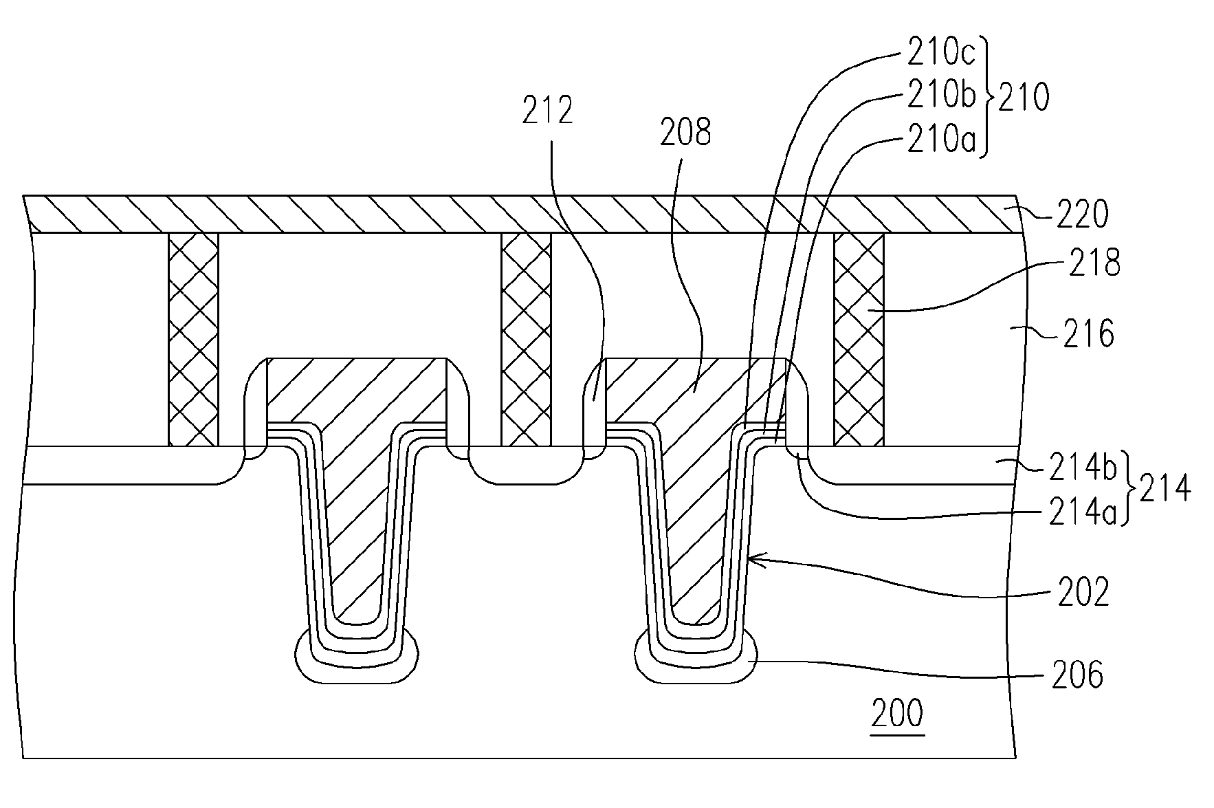
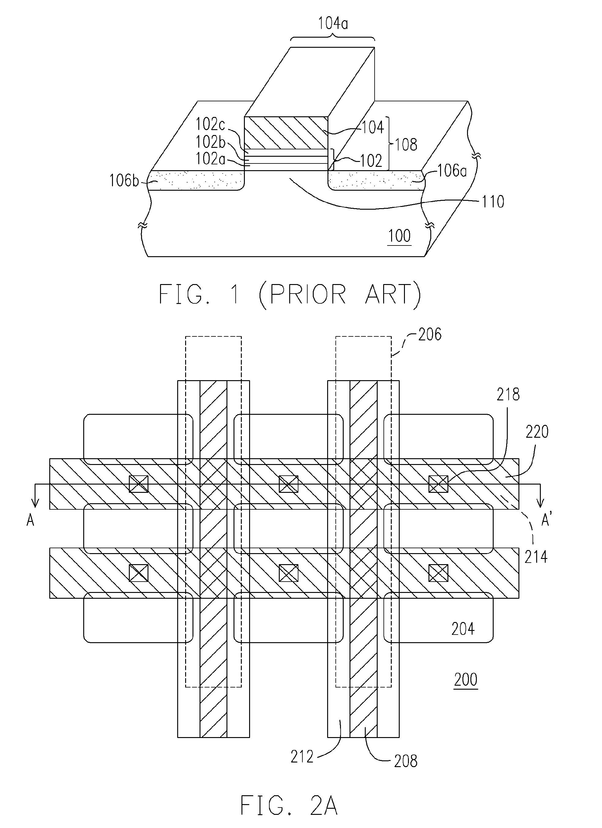
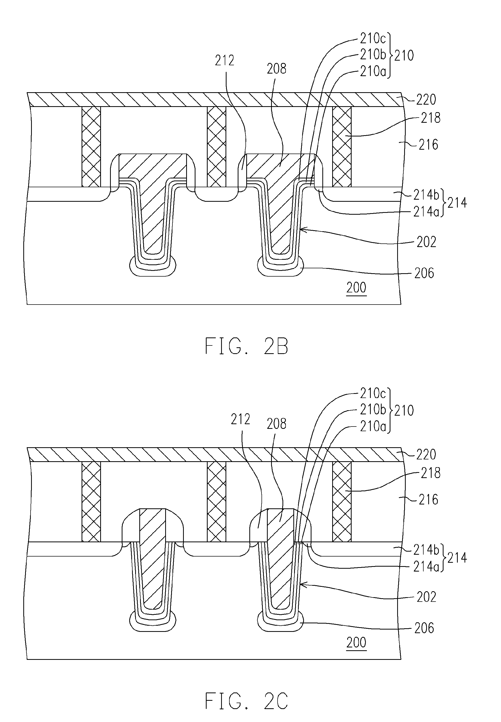
[0028]FIG. 2A is a top view showing the structure of a non-volatile memory cell according to one embodiment of the present invention. FIG. 2B is a schematic cross-sectional view of the non-volatile memory cell taken along line A–A″ of FIG. 2A. As shown in FIGS. 2A and 2B, the structure of the non-volatile memory cell includes a substrate 200, a device isolation structure 204, a source / drain region 206, a gate 208, a composite dielectric layer 210, a spacer 212, a source / drain region 214, an inter-layer dielectric layer 216, a contact plug 218 and a conductive line 220.

[0029]The substrate 200 is a silicon substrate, for example. The trench 202 is formed within the substrate 200. The device isolation s...


PUM


Abstract

A non-volatile memory cell is provided. The non-volatile memory at least includes a substrate, a gate, a first source / drain region, a composite dielectric layer and a second source / drain region. A trench is formed in a substrate and a gate is formed inside the trench. The first source / drain region is formed at the bottom of the trench. The composite dielectric layer is formed between the gate and the surface of the trench. The composite dielectric layer includes at least a charge-trapping layer. The second source / drain region is formed in the substrate next to the sides of the gate.

Description

CROSS REFERENCE TO RELATED APPLICATIONS[0001]This application claims the priority benefit of Taiwan application serial no.92137266, filed on Dec. 29, 2003.BACKGROUND OF INVENTION[0002]1. Field of the Invention[0003]The present invention relates to a semiconductor memory device. More particularly, the present invention relates to a non-volatile memory cell and manufacturing method thereof.[0004]2. Description of the Related Art[0005]Among various types of non-volatile memory products, electrically erasable programmable read-only memory (EEPROM) is a memory device that allows multiple data writing, reading and erasing operations. In addition, the stored data will be retained even after power to the device is removed. With these advantages, it has been broadly applied in personal computer and other electronic equipment. A typical EEPROM has a polysilicon floating gate and a polysilicon control gate. To program data into the memory device, electrons are injected into the floating gate. ...

Claims


Application Information

Patent Timeline
Patent Type & Authority Patents(United States)
IPC IPC(8): H01L29/788H01L21/336H01L21/8246H01L27/115H01L29/792
CPCH01L27/115H01L29/7926H01L29/792H01L27/11568H10B69/00H10B43/30
Inventor CHANG, KO-HSINGHUANG, CHIU-TSUNG
Owner POWERCHIP SEMICON MFG CORP
Why Eureka
Try Eureka