Non-volatile memory device and method of manufacturing the same

a memory device and non-volatile technology, applied in the direction of semiconductor devices, electrical devices, transistors, etc., can solve the problems of leakage current generation, overall storage capacity affect, reliability of the device, etc., and achieve the effect of improving the coupling ratio of the device and improving the storage efficiency of the memory devi

Active Publication Date: 2006-08-15
POWERCHIP SEMICON MFG CORP
View PDF5 Cites 15 Cited by
  • Summary
  • Abstract
  • Description
  • Claims
  • Application Information

AI Technical Summary

Benefits of technology

[0010]At least a second objective of this invention is to provide a non-volatile memory device with a smaller dimension but a higher coupling ratio so that overall storage efficiency of the device is improved.
[0013]Because the non-volatile memory device is fabricated within a trench in this invention, the coupling ratio of the device can be increased under the same device dimension so that the storage efficiency of the memory device is improved. Furthermore, depth of the trench is adjustable so that more charges can be stored inside the non-volatile memory device. In other words, the threshold voltage (Vt) for programming data can be changed by adjusting the depth of the trench. In addition, the process for fabricating the non-volatile memory is a single polysilicon process and hence is also applicable in an embedded process.

Problems solved by technology

Obviously, if the tunneling oxide layer underneath the polysilicon floating gate contains some defects, a leakage current will be produced and reliability of the device will be affected.
When the contact area between the top oxide layer and the polysilicon gate inside the SONOS memory device is reduced, overall storage capacity is affected.

Method used


Image

  • Non-volatile memory device and method of manufacturing the same
  • Non-volatile memory device and method of manufacturing the same
  • Non-volatile memory device and method of manufacturing the same

Examples


Embodiment Construction

[0019]Reference will now be made in detail to the present preferred embodiments of the invention, examples of which are illustrated in the accompanying drawings. Wherever possible, the same reference numbers are used in the drawings and the description to refer to the same or like parts.

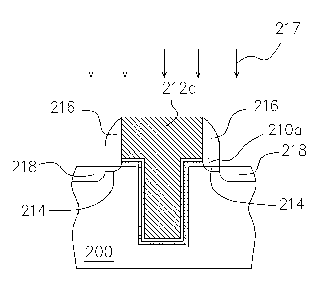
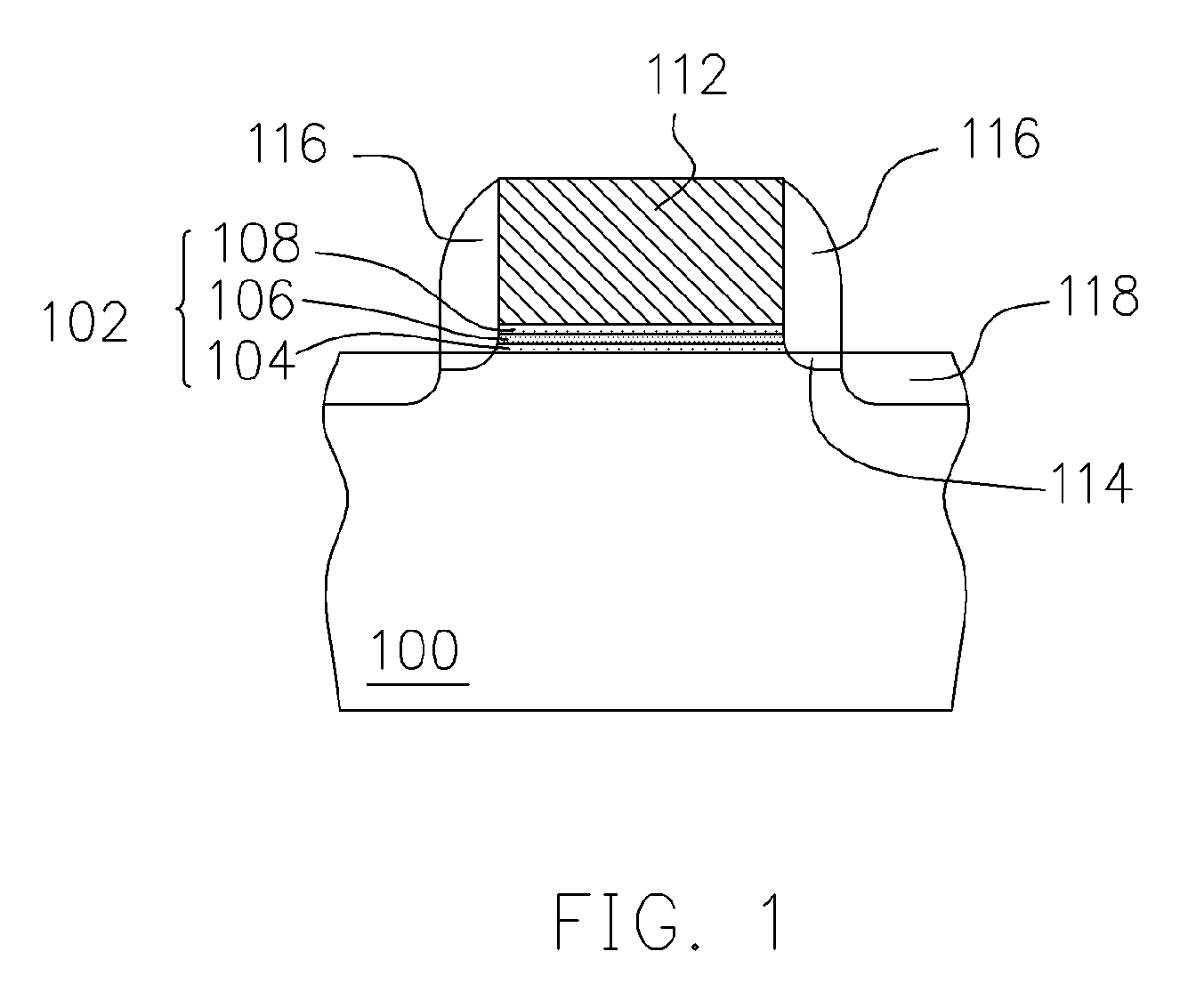
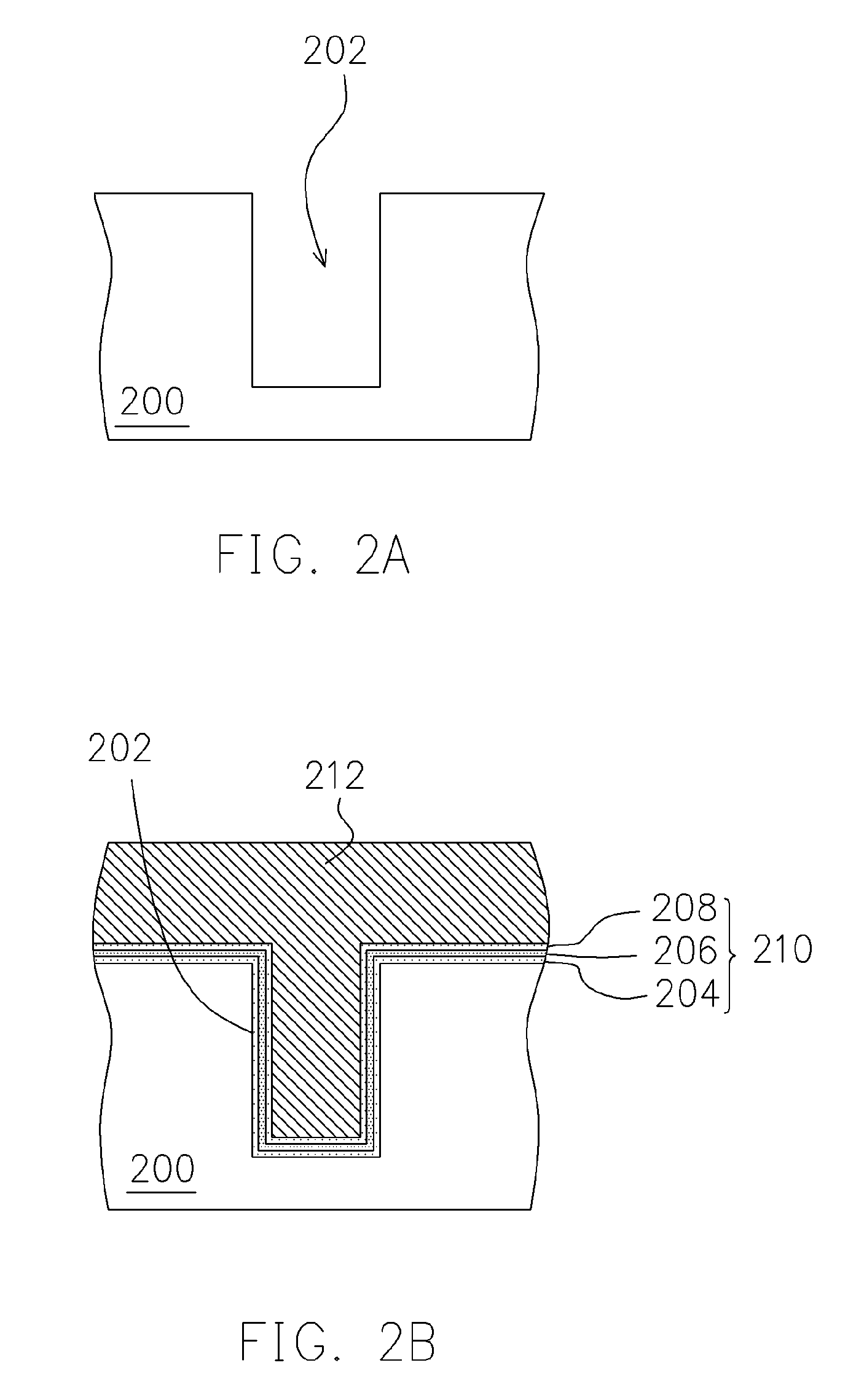
[0020]FIGS. 2A through 2D are schematic cross-sectional views showing the progression of steps for fabricating a non-volatile memory device according to one preferred embodiment of this invention. As shown in FIG. 2A, a substrate 200 is provided. Thereafter, a trench 202 is formed in the substrate 200. To form the trench 202, a pad oxide layer (not shown) is first formed over the substrate 200. A patterned mask layer (not shown) fabricated from silicon nitride or other suitable material is next formed over the pad oxide layer. Using the patterned mask layer as a mask, the exposed pad oxide layer and a portion of the substrate 200 is removed. Finally, the pad oxide layer and the patterned mask layer a...


PUM


Abstract

A non-volatile memory device and method of manufacturing the same is provided. A substrate is provided and then a trench is formed in the substrate. Thereafter, a bottom oxide layer, a charge-trapping layer and a top oxide layer are sequentially formed over the substrate and the surface of the trench. A conductive layer is formed over the top oxide layer filling the trench. The conductive layer is patterned to form a gate over the trench. The top oxide layer, the charge-trapping layer and the bottom oxide layer outside the gate are removed. A source / drain doping process is carried out. Because the non-volatile memory device is manufactured within the trench, storage efficiency of the device is improved through an increase in the coupling ratio. Furthermore, more charges can be stored by increasing the depth of the trench.

Description

BACKGROUND OF INVENTION[0001]1. Field of the Invention[0002]The present invention relates to a memory device and manufacturing method thereof. More particularly, the present invention relates to a non-volatile memory device and method of manufacturing the same.[0003]2. Description of the Related Art[0004]Electrically erasable programmable read-only memory (EEPROM) is a non-volatile memory device that allows multiple data writing, reading, and erasing operations. In addition, the stored data will be retained even after power to the device is removed. With these advantages, it has been broadly applied in personal computer and electronic equipment. A typical EEPROM device has a floating gate and a control gate fabricated using doped polysilicon. During a programming operation, electrons injected into the floating gate will be evenly distributed over the entire polysilicon floating gate layer. Obviously, if the tunneling oxide layer underneath the polysilicon floating gate contains some...

Claims


Application Information

Patent Timeline
Patent Type & Authority Patents(United States)
IPC IPC(8): H01L21/336H01L21/28H01L29/423H01L29/51H01L29/792
CPCH01L29/513H01L29/792H01L29/78H01L21/28194H01L21/28202H01L29/518H01L29/517
Inventor HSU, HANN-JYECHANG, KO-HSING
Owner POWERCHIP SEMICON MFG CORP
Why Eureka
Try Eureka