Systems and methods for handling immediate data errors in flash memory

a flash memory and error handling technology, applied in the direction of memory address/allocation/relocation, instruments, coding, etc., can solve the problems of detection errors, bit error rate, and decrease of device reliability, so as to increase the bit error rate, enhance the effect of inaccuracy effects, and high density

Active Publication Date: 2010-05-13
AVAGO TECH INT SALES PTE LTD
View PDF14 Cites 108 Cited by
  • Summary
  • Abstract
  • Description
  • Claims
  • Application Information

AI Technical Summary

Benefits of technology

[0009]Today's Flash memory devices store information with high density on Flash cells with ever smaller dimensions. In addition, Multi-Level Cells (MLCs) store several bits per cell by differentially setting the amount of charge in the cell. The amount of charge is then measured by a detector, e.g. in the form of a threshold voltage of the transistor gate. Due to inaccuracies during the programming procedure and charge loss due to retention in memory and temperature, the measured levels during a Read operation suffer from detection errors. The small dimensions of the Flash cells result in cells that can store very small amounts of charge, enhancing the effects of inaccuracies due to randomness of programming, retention and previous erase / write cycles. Thus, new single level cells (SLC) and multi-level cell devices have significantly increased bit error rate (BER), decreasing the reliability of the device.

Problems solved by technology

Due to inaccuracies during the programming procedure and charge loss due to retention in memory and temperature, the measured levels during a Read operation suffer from detection errors.
Thus, new single level cells (SLC) and multi-level cell devices have significantly increased bit error rate (BER), decreasing the reliability of the device.
An important factor of flash memory cost is the proportion of space allocated to “spare bits”, especially redundant information used to correct read errors e.g. due to retention.

Method used


Image

  • Systems and methods for handling immediate data errors in flash memory
  • Systems and methods for handling immediate data errors in flash memory
  • Systems and methods for handling immediate data errors in flash memory

Examples


second embodiment

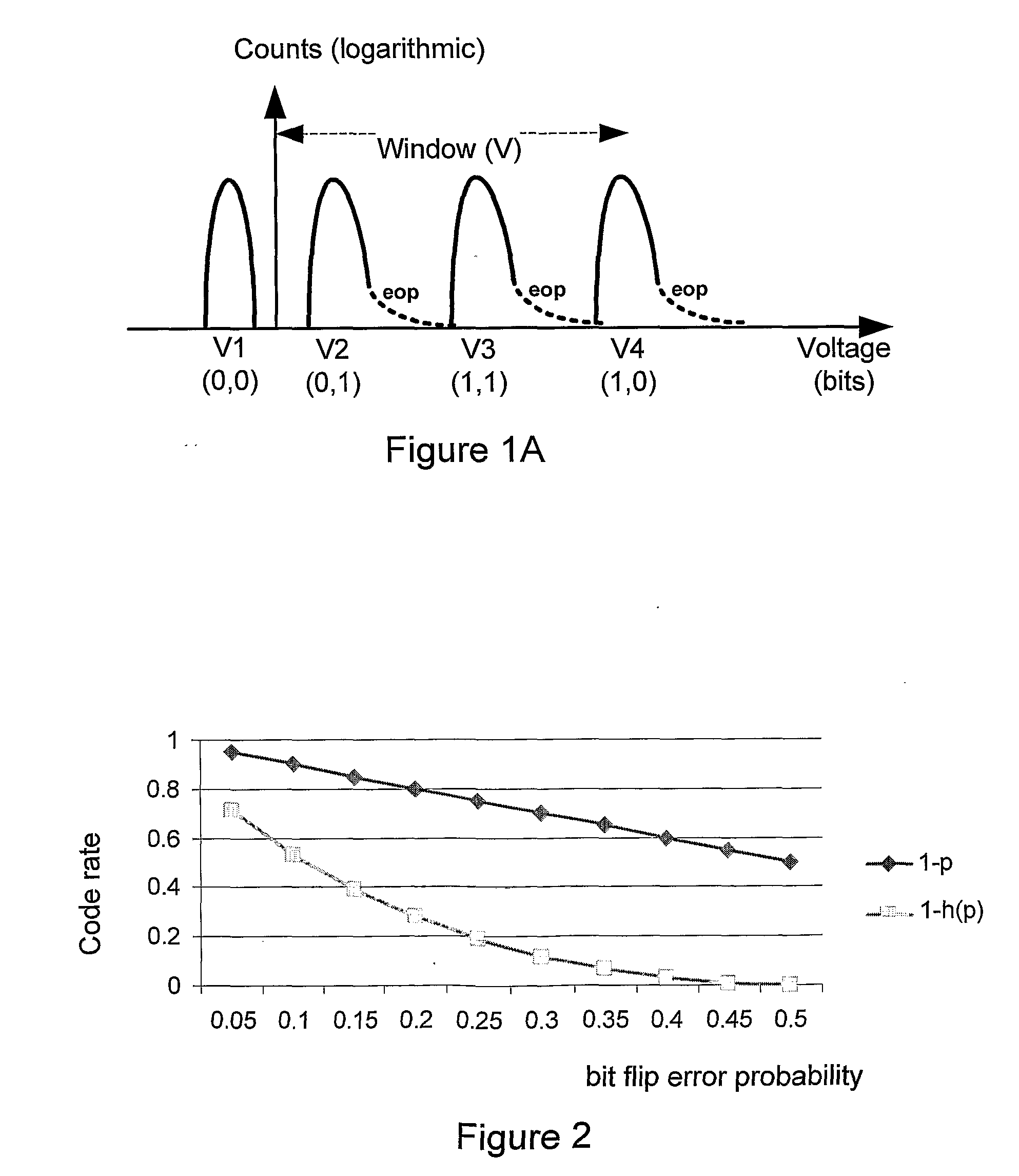
[0067]A second embodiment, as shown in FIG. 3, is to allocate an additional program level which will be denoted as an erasure level at each program symbol. The erasure symbols may be denoted by the top program level. The locations of erratic over-programming are then marked by doing a second programming procedure which raises the program levels of the erratic over-programming locations to the top level. FIG. 3 is an example of a case of a multi-level cell with 4 program levels and one erasure level marked as V5. More generally, a region between any two program levels may be deemed an erasure region. The program window may be divided into multiple erasure regions interspersed with multiple symbol regions figures shown in FIG. 3. In FIG. 3, by way of example, there are four erasure regions marked E1, E2, E3 and E4. The levels are tuned according to the erasure coding capability. If a specific cell's programmed level lies in the erasure region above it, or in any of the regions above t...

first embodiment

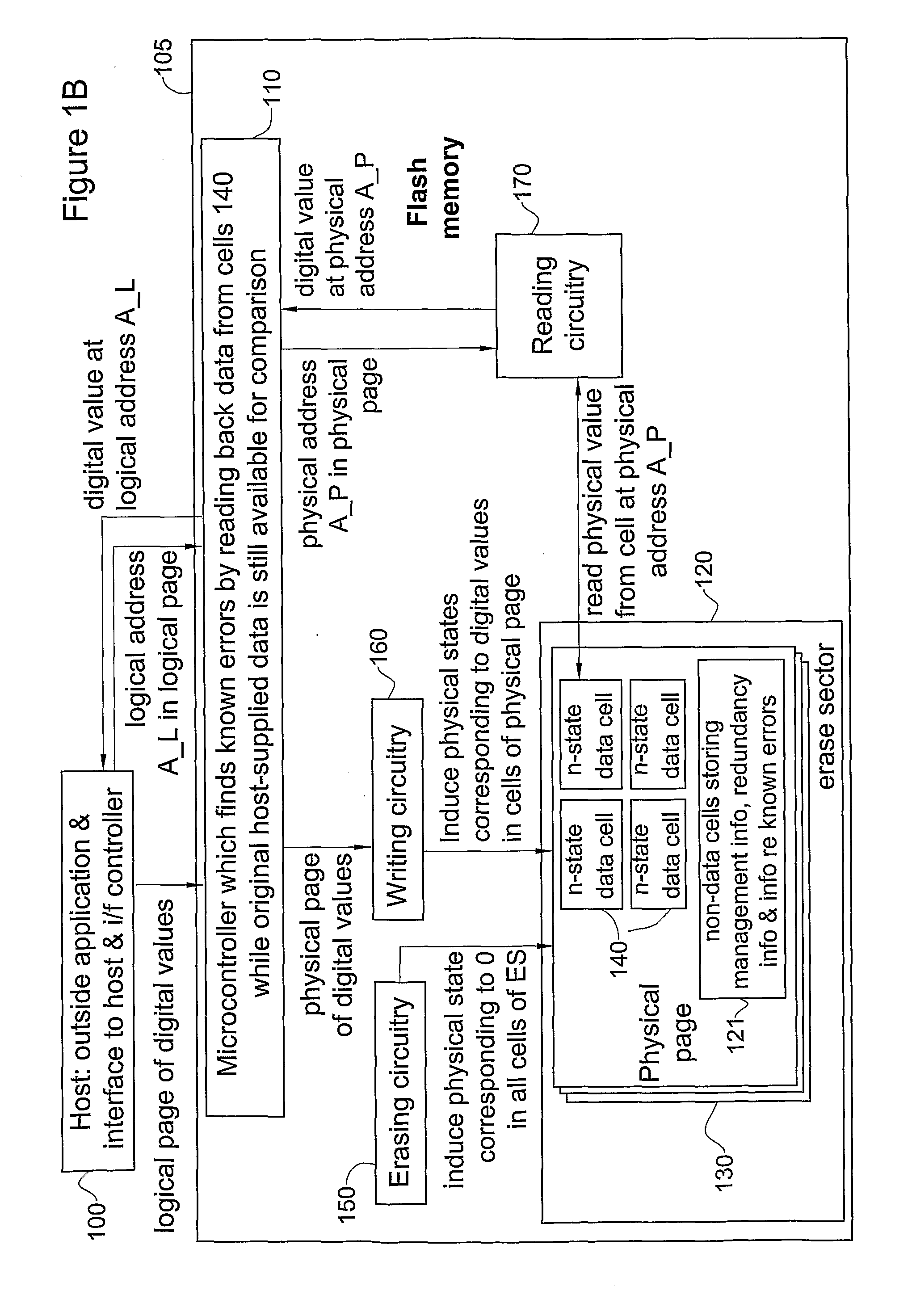
[0070]FIG. 1B is a simplified functional block diagram of a flash memory system constructed and operative, in accordance with the present invention, to identify and rectify data errors which occur while the temporary memory from which the data was read, still exists. As shown, the system of FIG. 1C includes a host 100 interfacing with a flash memory device 105 including a microcontroller 110 (some or all of whose functions may alternatively be performed by an external microcontroller connected between the flash memory and the host), and one or more erase sectors 120 each having one or more physical pages 130 each of which comprises a plurality of data cells 140 as well as non-data cells 121. Also included is erasing circuitry 150, writing circuitry 160 and reading circuitry 170. The microcontroller 110 finds known errors by reading back data from cells 140 while original host-supplied data is still available for comparison. The non-data cells 121 are operative to store management in...

third embodiment

[0072]FIG. 1D is a simplified functional block diagram of a flash memory system constructed and operative, in accordance with the present invention, to identify and rectify data errors which occur while the temporary memory, from which the data was read, still exists. In the embodiment of FIG. 1D, the microcontroller 110, or an external controller, finds known errors by reading back data from cells 140 while original host-supplied data is still available for comparison, re-writes data replacing known errors with dummy values and appending correct values, and, during reading, replaces dummy values with appended correct values. Non-data cells 121 typically store management info, redundancy info and content for cells found to be in dummy state, all as described in detail below with reference to FIGS. 9-10. In this embodiment, the data cells 140 have n data states plus one additional dummy state earmarking cell as suffering from known error.

[0073]A first embodiment of erratic over-progr...


PUM


Abstract

A flash memory system comprising temporary memory, writing apparatus for writing first logical data from the temporary memory into flash memory cells having at least two levels, thereby to generate a physical representation of the first logical data including known errors, reading apparatus for reading the physical representation from the cells, thereby to generate, and store in the temporary memory, second logical data which if read immediately is identical to the first logical data other than the known errors; and controlling apparatus controlling the writing apparatus and the reading apparatus and including known error ID apparatus operative to identify the known errors by comparing the first logical data to second logical data read immediately after the physical representation is generated, to store information characterizing the known errors and to use the information, when the second logical data is next read, to correct the known errors.

Description

REFERENCE TO CO-PENDING APPLICATIONS[0001]Priority is claimed from the following co-pending applications: U.S. Provisional Application No. 61 / 006,806, filed Jan. 31, 2008 and entitled “Systems and Methods for using a Erasure Coding in Flash memory” and U.S. Provisional Application No. 61 / 071,486, filed May 1, 2008 and entitled “Systems and Methods for Handling Immediate Data Errors in Flash Memory”.[0002]Other co-pending applications include: U.S. Provisional Application No. 60 / 960,207, filed Sep. 20, 2007 and entitled “Systems and Methods for Coupling Detection in Flash Memory”, U.S. Provisional Application No. 61 / 071,467, filed Apr. 30, 2008 and entitled “Improved Systems and Methods for Determining Logical Values of Coupled Flash Memory Cells”, U.S. Provisional Application No. 60 / 960,943, filed Oct. 22, 2007 and entitled “Systems and methods to reduce errors in Solid State Disks and Large Flash Devices” and U.S. Provisional Application No. 61 / 071,469, filed Apr. 30, 2008 and enti...

Claims


Application Information

Patent Timeline
Patent Type & Authority Applications(United States)
IPC IPC(8): G06F11/14G06F11/07G06F12/02
CPCG06F11/1072G11C11/5628G11C16/14G11C16/3404G11C2211/5621G11C16/3454G11C16/3463G11C16/3486G11C29/00G11C16/3413
Inventor WEINGARTEN, HANANLEVY, SHMUEL
Owner AVAGO TECH INT SALES PTE LTD
Why Eureka
Try Eureka