Driver circuit and liquid crystal display device

a technology of driving circuit and liquid crystal display device, which is applied in the direction of logic circuit coupling/interface arrangement, instruments, computing, etc., can solve the problem of inability to carry out the fixation of buffers conforming to specific video digital data(some specific grayscale level) and cannot be carried ou

Inactive Publication Date: 2005-06-21
RENESAS ELECTRONICS CORP
View PDF3 Cites 51 Cited by
  • Summary
  • Abstract
  • Description
  • Claims
  • Application Information

AI Technical Summary

Benefits of technology

[0020]A driver circuit, in accordance with further aspect of the present invention, comprises: first and second buffer circuits having respective ones of input terminals connected commonly to one input terminal provided for receiving an input signal voltage and respective ones of output terminals connected commonly to an output terminal, the first buffer circuit having an operating range at least on the side of a high potential and the second buffer circuit having an operating range at least on the side of a low potential; reference voltage generating means for generating a reference voltage corresponding to a voltage range in which both the first and second buffer circuits are capable of operating; and a comparator for comparing the reference voltage, which is output from the reference voltage generating means, and the input signal voltage; wherein the first buffer circuit and the second buffer circuit have their activation and deactivation controlled based upon an output signal of the comparator, which indicates result of the comparison, and a control signal.
[0020]A driver circuit, in accordance with further aspect of the present invention, comprises: first and second buffer circuits having respective ones of input terminals connected commonly to one input terminal provided for receiving an input signal voltage and respective ones of output terminals connected commonly to an output terminal, the first buffer circuit having an operating range at least on the side of a high potential and the second buffer circuit having an operating range at least on the side of a low potential; reference voltage generating means for generating a reference voltage corresponding to a voltage range in which both the first and second buffer circuits are capable of operating; and a comparator for comparing the reference voltage, which is output from the reference voltage generating means, and the input signal voltage; wherein the first buffer circuit and the second buffer circuit have their activation and deactivation controlled based upon an output signal of the comparator, which indicates result of the comparison, and a control signal.

Problems solved by technology

A problem that arises in such cases is that a fixed changeover between buffers conforming to some specific video digital data(some specific grayscale level) cannot be carried out.

Method used


Image

  • Driver circuit and liquid crystal display device
  • Driver circuit and liquid crystal display device
  • Driver circuit and liquid crystal display device

Examples


Embodiment Construction

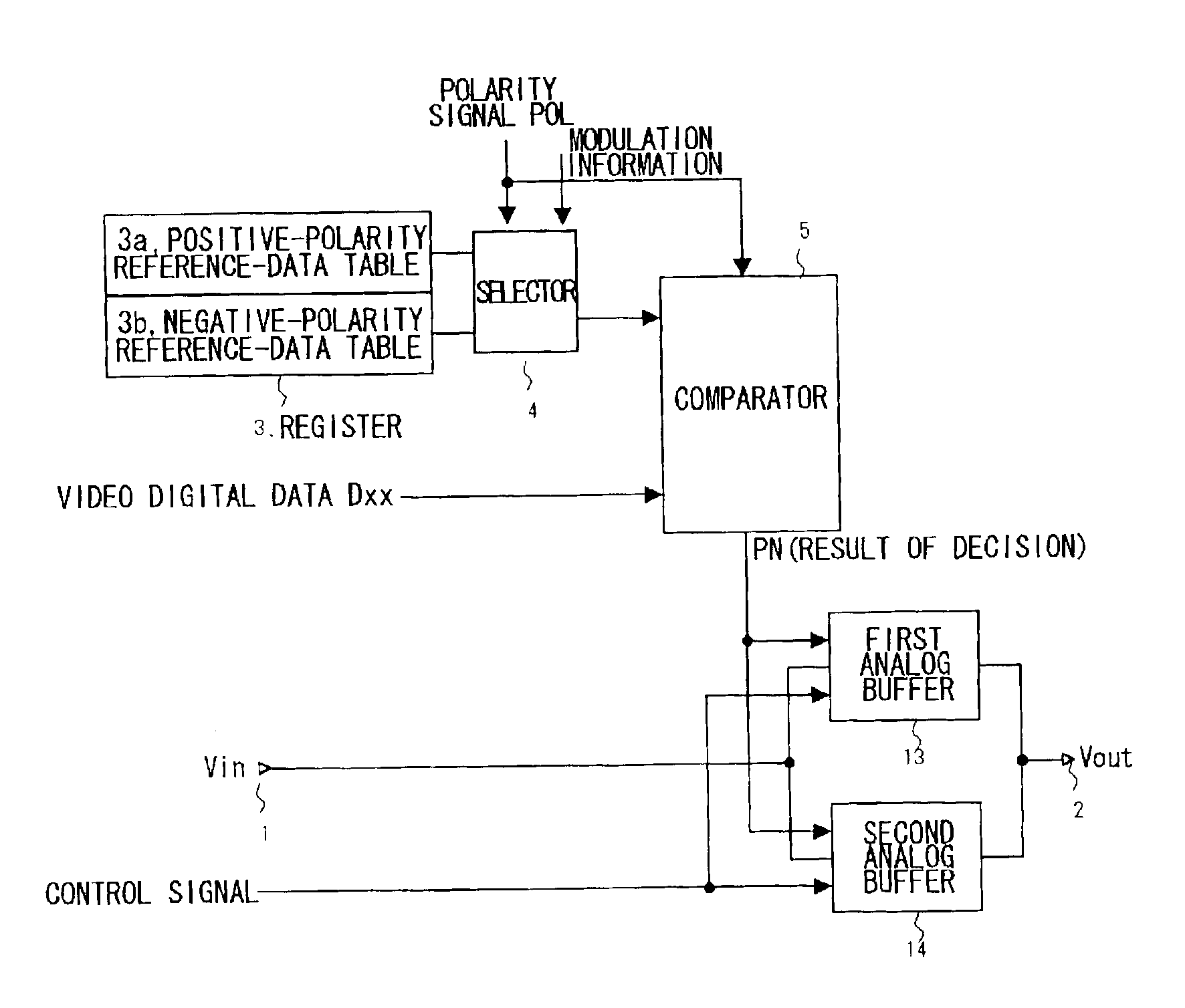
[0049]Preferred embodiments of the present invention will be described below.

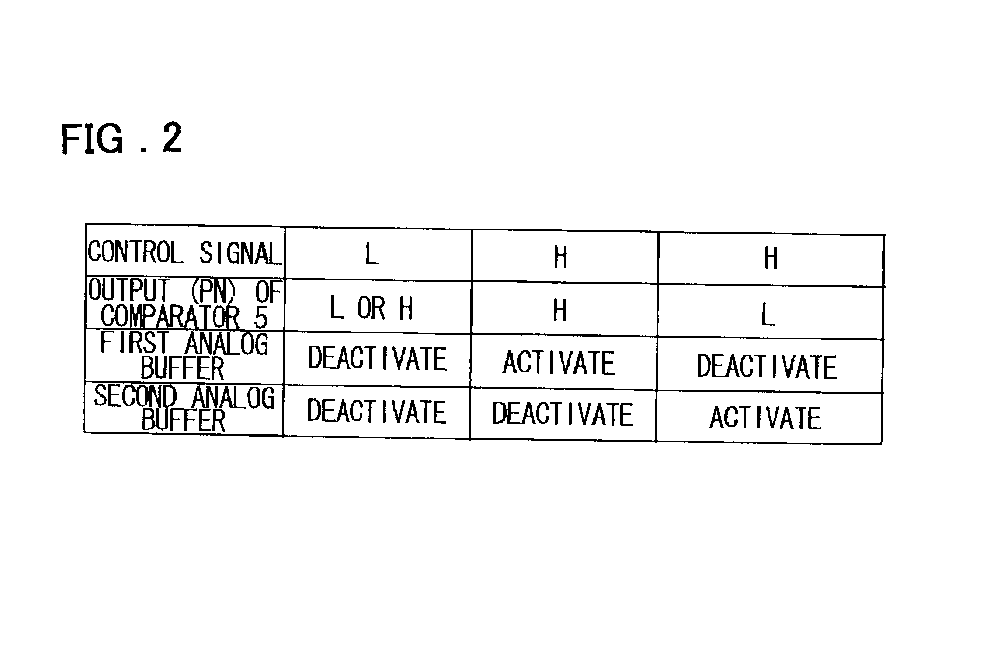
[0050]The present invention provides a driver circuit which, even if individual analog buffers thereof cannot produce a full-range output, is capable of providing a full-range output by switching between the two buffers. The optimum one of the two buffers is selected to make possible normal drive at all times even when various types of modulation are applied, Specifically, modulation of a variety of conditions is divided into a plurality of steps, and a table is provided for storing digital data, which corresponds to a grayscale level at which the two buffers are changed over, on a per-modulation-step basis The data in the table is adopted as reference data and is compared with video digital data, and the optimum buffer is selected based upon the result of the comparison.

[0051]A voltage that resides in a range in which the two buffers are capable of being changed over is adopted as a reference voltage with ...


PUM

PropertyMeasurementUnit
voltageaaaaaaaaaa
voltageaaaaaaaaaa
voltageaaaaaaaaaa

Abstract

Disclosed is a driver circuit, as well as a LCD device having the driver circuit, in which changeover between first and second buffer circuits the operating ranges of which extend to high- and low-potential power supply voltages can be performed reliably within the drive changeover range. The driver circuit includes first and second buffer circuits having their input terminals connected in common with one input terminal to which an input signal voltage is input and having their output terminals connected in common with an output terminal, the first and second buffer circuits having operating ranges that extend to high- and low-potential power supply voltages, respectively; first and second storage units for storing respectively positive- and negative-polarity reference data, which correspond to voltages within a range in which both of the first and second buffer circuits are operable, with regard to each of a standard state and modulated state of a gamma characteristic; a selector for selecting either of the storage units based upon a polarity signal, and selectively outputting reference data corresponding to the standard or modulated state based upon modulation information that specifies modulation; and a comparator for comparing entered data and the reference data output from the selector. Activation and deactivation of the first and second buffer circuits is controlled based upon an output signal from the comparator and a control signal.

Description

FIELD OF THE INVENTION[0001]This invention relates to a driver circuit and, more particularly, to a driver circuit suited for driving a capacitative load.BACKGROUND OF THE INVENTION[0002]For technical publications related to the present invention, see (1) the reference “A New Low-Power Driver for Portable Devices,” by H. Tsuchi, N. Ikeda and H. Hayama, SID 00 DIGEST pp. 146-149, and (2) the specification of Japanese Patent Kokai Publication JP-A-2000-33846.[0003]FIG. 24 is a diagram illustrating one example of a driver circuit for driving video digital data in a liquid crystal display device [see FIG. 1 in reference (1)].[0004]The buffer shown in FIG. 24 is such that even if a full-range output cannot be produced with an analog buffer alone, a full-range output is made possible by switching between two analog buffer circuits (referred to simply as “buffer circuits” below) The term “full-range output” refers to substantially the entire area of the range of power supply voltage of the...

Claims


Application Information

Patent Timeline
Patent Type & Authority Patents(United States)
IPC IPC(8): G09G3/36G09G3/20H03K19/0175G02F1/133
CPCG09G3/3688G09G3/3614G09G2310/0291G09G2310/0248G09G2310/027G09G3/3696
Inventor TSUCHI, HIROSHIUCHIYAMA, YOSHINORI
Owner RENESAS ELECTRONICS CORP
Why Eureka
Try Eureka