Electro-optic modulators with internal impedance matching

a technology of impedance matching and optical modulator, applied in optics, instruments, optical light guides, etc., can solve the problems of low reliability above 1-1.5 ghz, unreliable impedance matching between the rf signal source and the device, and the impedance value of the integrated modulator. achieve the effect of compact layou

Inactive Publication Date: 2005-06-21
OCLARO NORTH AMERICA
View PDF13 Cites 9 Cited by
  • Summary
  • Abstract
  • Description
  • Claims
  • Application Information

AI Technical Summary

Benefits of technology

[0029]Applicants have further discovered that if the modulator is resonant, the matching network can be given a simple topology based on stub-line arrangements. In particular, the matching network may be placed between the modulator input and the coaxial connector, and may partially replace the constant impedance transition.
[0030]Applicants have still further discovered that the final taper leading from the matching section to the coaxial transition can be either with a non-optimal impedance or can be given an impedance so as to provide an additional degree of freedom in the matching section. It can be used as part of the matching network itself. By proper design and use of internally matched planar waveguides, an extremely compact layout may be obtained, thus enabling full compatibility, in terms of mounting, dimensions and position of external connectors, with previous designs based on external impedance matching.
[0031]In one aspect, an optical transmission system according to the invention comprises: an optical source for generating an optical signal; an RF signal source for generating an RF signal at a predetermined frequency, the RF signal source having an impedance; a resonant optical phase modulator for modulating the phase of the optical signal according to the RF signal; an optical amplifier for amplifying the optical signal to a power greater than 6 dBm; an optical fiber line for transmitting the amplified and phase modulated optical signal. The resonant optical phase modulator includes: an electro-optical substrate; an optical waveguide formed in the substrate and having a variable index of refraction; an active modulator electrode formed on the substrate in relation to the waveguide to effect electro-optical variation of the index of refraction upon application to the electrode of a modulating signal; an interface port formed on the substrate and providing the RF modulating signal to the electrode; an electrical structure, formed on the substrate and coupled to the interface port and the electrode, an impedance of the optical modulator including the interface port and the electrical structure being substantially equal to the impedance of the RF signal source.
[0032]In another aspect, a resonant optical modulator consistent with the invention includes an electro-optical substrate, an optical waveguide formed in the substrate and having a variable index of refraction, and a resonant active modulator electrode formed on the substrate in relation to the waveguide to effect electro-optical variation of the index of refraction upon application to the electrode of a modulating signal at a frequency around a resonant frequency. The modulator also includes an interface port formed on the substrate which provides the modulating signal to the electrode from a signal source, which has an impedance, and an electrical structure, formed on the substrate and coupled to the interface port and the electrode, for making an impedance of the optical modulator substantially equal to the impedance of the signal source.

Problems solved by technology

Applicants have noticed that external matching, e.g., the simple integration within the package of a circuit comprising concentrated elements, such as capacitors, resistors and / or inductors, results in a very low reliability above 1-1.5 GHz.
In such a case, the parasitic impedances induced by the strips used for soldering the concentrating elements in a circuit can cause a shift in the expected resonance frequency, resulting in an unpredictable impedance value for the integrated modulator and in an unreliable impedance matching between the RF signal source and the device.

Method used


Image

  • Electro-optic modulators with internal impedance matching
  • Electro-optic modulators with internal impedance matching
  • Electro-optic modulators with internal impedance matching

Examples


Embodiment Construction

[0064]Reference will now be made to various embodiments according to this invention, examples of which are shown in the accompanying drawings and will be obvious from the description of the invention. In the drawings, the same reference numbers represent the same or similar elements in the different drawings whenever possible.

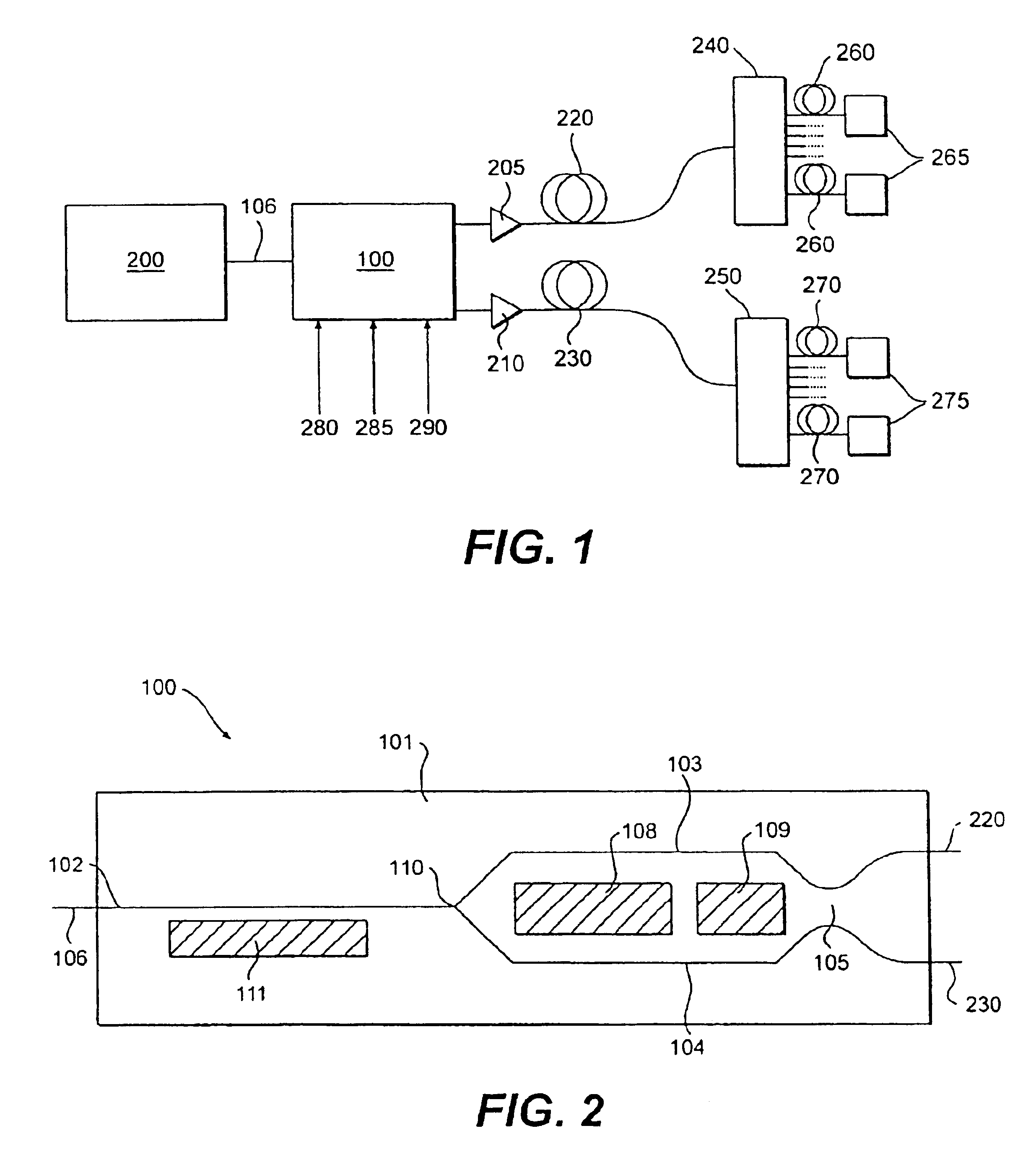
[0065]A CATV transmission system according to the invention is schematically shown in FIG. 1. The output of a laser source 200, such as a semiconductor laser source (e.g., a DFB laser), is coupled via a single mode optical fiber 106 to the input of an electro-optical modulator 100. Typical wavelength values for the laser source 200 are, for example, in the range 1540-1560 nm or in the range 1300-1320 nm. Fiber 106 is preferably a polarization maintaining fiber.

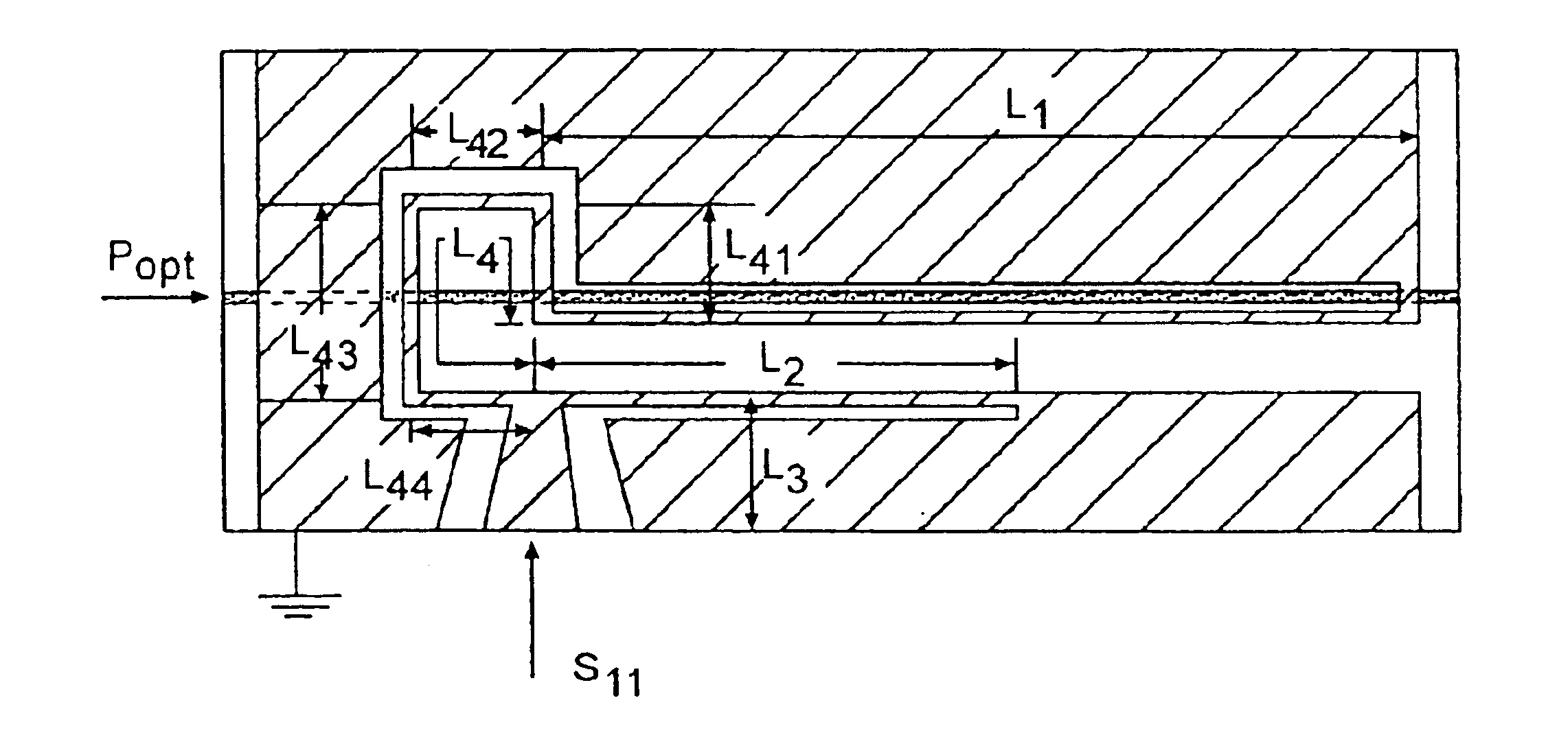
[0066]The optical modulator 100, which is particularly adapted for use in CATV systems, is schematically shown in FIG. 2. The modulator 100 is formed on a planar substrate 101. On the substrate surface, a...


PUM

PropertyMeasurementUnit
impedanceaaaaaaaaaa
impedanceaaaaaaaaaa
resonance frequencyaaaaaaaaaa

Abstract

A resonant optical modulator includes an electro-optical substrate, an optical waveguide formed in the substrate and having a variable index of refraction, and an active modulator electrode formed on the substrate in relation to the waveguide to effect electro-optical variation of the index of refraction upon application to the electrode of a modulating signal. An interface port formed on the substrate provides the modulating signal to the electrode from a signal source and has an impedance. An electrical structure, formed on the substrate and coupled to the interface port and the electrode, makes an impedance of the optical modulator substantially equal to the impedance of the signal source. The electrical structure includes a delay line and a stub formed on the substrate.

Description

CROSS-REFERENCE TO RELATED APPLICATIONS[0001]This application is a divisional of U.S. patent application Ser. No. 09 / 610,437, filed Jul. 3, 2000 now U.S. Pat. No. 6,763,151, which claims benefit of U.S. provisional patent application Ser. No. 60 / 144,626, filed Jul. 20, 1999 and Europe Patent Application No. 99 112827.3, filed Jul. 2, 1999. Each of the aforementioned related patent applications is herein incorporated by reference.BACKGROUND OF THE INVENTION[0002]The present invention relates generally to electro-optic modulators and, more particularly, to optical modulators having an internal structure for matching impedance with coaxial connectors.[0003]The operation of electro-optic modulators is based on the interaction between an electrical microwave, or radio frequency (RF), modulating signal and an optical signal. An optical modulator is typically obtained by utilizing the electro-optical effect of the modulator's waveguide material. This effect comprises changing, through an a...

Claims


Application Information

Patent Timeline
Patent Type & Authority Patents(United States)
IPC IPC(8): G02F1/035G02F1/01G02F1/225
CPCG02F1/0356G02F2201/125G02F1/2255
Inventor BOSSO, SERGIOCASACCIA, EMILIOFRASSATI, DAVIDEGHIONE, GIOVANNIPERASSO, ALDOPIROLA, MARCO
Owner OCLARO NORTH AMERICA
Why Eureka
Try Eureka