Turn-on characteristic testing apparatus of large power semiconductor device

A characteristic test and semiconductor technology, applied in the field of power electronics, can solve problems such as economic losses and potential safety hazards, and achieve the effects of comprehensive functions, high reliability, and improved test accuracy

Active Publication Date: 2013-04-17
CHINA EPRI ELECTRIC POWER ENG CO LTD +2
View PDF4 Cites 17 Cited by
  • Summary
  • Abstract
  • Description
  • Claims
  • Application Information

AI Technical Summary

Problems solved by technology

Since high-power semiconductor devices are usually used under demanding working conditions, any damage to the device will cause safety hazards and economic losses. In order to ensure the safe and reliable operation of the device, it is necessary to test the performance indicators and parameters of all aspects of the device used. Understand the device characteristics in detail and judge whether it can meet the needs of actual working conditions

Method used


Image

  • Turn-on characteristic testing apparatus of large power semiconductor device
  • Turn-on characteristic testing apparatus of large power semiconductor device
  • Turn-on characteristic testing apparatus of large power semiconductor device

Examples


Embodiment Construction

[0022] The present invention will be described in further detail below in conjunction with the accompanying drawings.

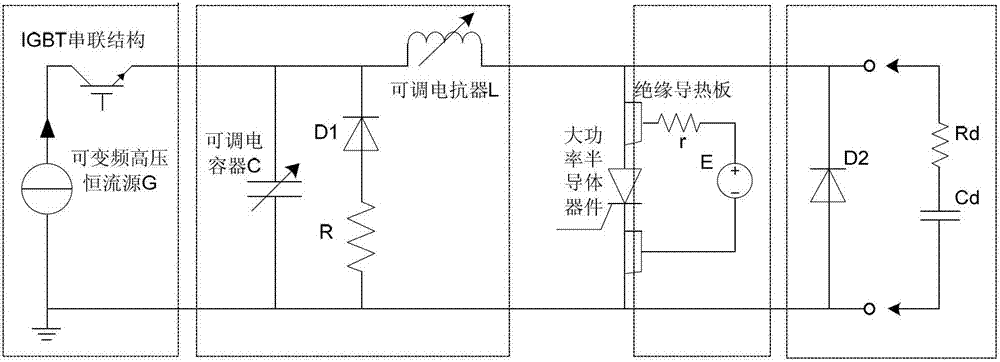
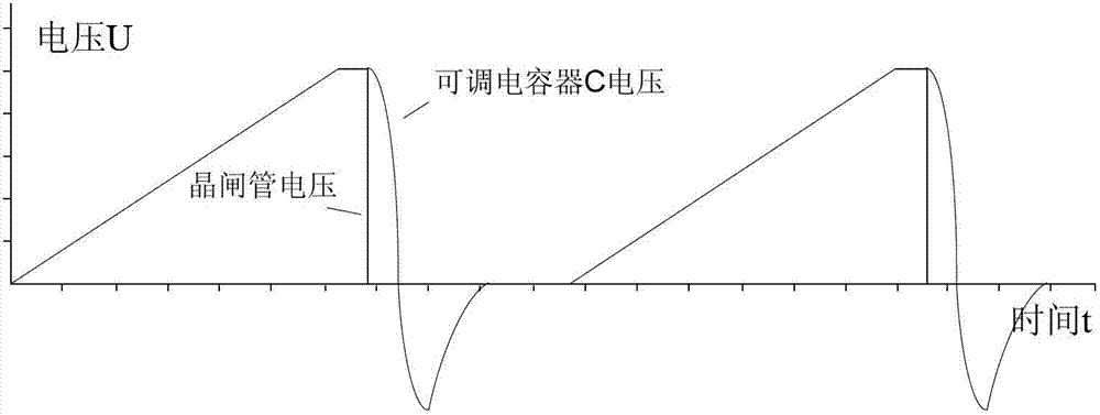
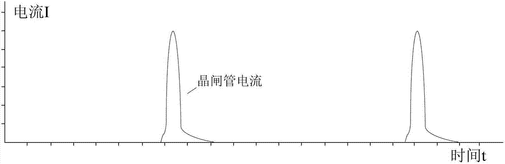
[0023] Such as Figure 1-Figure 3 , the present invention provides a high-power semiconductor device turn-on characteristic test device, the device includes a constant current source unit, a test main circuit unit, a heating circuit unit and a protection circuit unit; the test main circuit unit includes an adjustable capacitor C, a damping The R-D1 branch and the adjustable reactor L formed by the resistance R and the diode D1 in series; the constant current source unit outputs a direct current to charge the adjustable capacitor C, and the adjustable capacitor C is charged to the test voltage. The discharge and the adjustable reactor L resonate to generate a test current to realize the opening test of the high-power semiconductor device under different working conditions; the heating circuit unit heats the high-power semiconductor device to the test junction ...


PUM


Abstract

The invention provides a turn-on characteristic testing apparatus of a large power semiconductor device. The turn-on characteristic testing apparatus of a large power semiconductor device comprises a constant current source unit, a testing main circuit unit, a heating loop unit and a protective loop unit, wherein the constant current source unit outputs direct current and can charge an adjustable capacitor C; the adjustable capacitor C is charged to reach a testing voltage; in the course of discharging, the adjustable capacitor C generates a testing current with an adjustable electric reactor L in a resonance oscillation way; in such a way, a turn-on test on the large power semiconductor device under various working conditions is realized; the heating loop circuit heats the large power semiconductor device to a testing junction temperature; and the protective loop unit prevents damages to the large power semiconductor device caused by the test. With the adoption of the turn-on characteristic testing apparatus of a large power semiconductor device, the turn-on test can be performed on the tested large power semiconductor device under the various conditions; the device is simple and practical in topological structure and comprehensive in function, and can satisfy the requirements of the turn-on characteristic test on the device under the various conditions; meanwhile, the protective measures for the device and the tested device in the case of faults are fully taken into account; and therefore, the reliability is high.

Description

technical field [0001] The invention belongs to the technical field of power electronics, and in particular relates to a high-power semiconductor device turn-on characteristic test device. Background technique [0002] Since the advent of silicon thyristors in the 1950s, for more than 50 years, researchers of power semiconductor devices have made unremitting efforts to achieve the ideal goal, and have achieved remarkable achievements. In the late 1960s, the turn-off thyristor GTO realized the gate turn-off function, and extended the chopper operating frequency to above 1KHZ. In the mid-1970s, high-power transistors and power MOSFETs came out, and power devices realized field control functions, opening the door to high-frequency applications. In the 1980s, the insulated gate bipolar transistor (IGBT) came out, which combined the functions of both power MOSFET and bipolar power transistor. Therefore, the current research work on power devices mainly focuses on the integratio...

Claims


Application Information

Patent Timeline
Patent Type & Authority Applications(China)
IPC IPC(8): G01R31/26
Inventor 雷小舟陈争光高冲王高勇
Owner CHINA EPRI ELECTRIC POWER ENG CO LTD
Why Eureka
Try Eureka