Cleaning and etching methods and their apparatuses

a technology of cleaning and etching, applied in the direction of cleaning using liquids, separation processes, instruments, etc., can solve the problems of difficult to remove the above-mentioned oil films, difficult to avoid the attachment of extremely minute silicon dust, and difficult to remove extremely minute silicon pieces, etc., to achieve the effect of difficult removal

Inactive Publication Date: 2005-07-05
SUMITOMO PRECISION PROD CO LTD
View PDF20 Cites 7 Cited by
  • Summary
  • Abstract
  • Description
  • Claims
  • Application Information

AI Technical Summary

Benefits of technology

[0009]It is an object of the present invention to provide a cleaning method and an apparatus therefor which, in the case of any of various apparatuses, a carrier or the like used in the manufacture of semiconductor wafers or semiconductor devices, are capable of removing minute silicon dust attached and accumulated inside the apparatuses, or removing by cleaning minute silicon pieces and grease that are conventionally difficult to remove.
[0012]Moreover, the present inventors discovered that if the above-mentioned vacuum atmosphere is made to contain a trace of water, then the H2O and the XeF2 in the atmosphere react with one another to produce HF, and hence for example an native oxide on silicon formed on the surface of silicon pieces or the like can be removed, and then subsequently the silicon can be etched through the XeF2 acting directly on the silicon in an atmosphere not containing water; the series of cleaning and etching reactions is extremely rapid, and hence cleaning and etching can be carried out in a reduced time.
[0013]Furthermore, the present inventors discovered that if the two steps are carried out in succession, i.e. the amount of SiO2 oxide film formed on silicon pieces to be removed is estimated, a prescribed amount of water is made to remain behind in or is added to the atmosphere, and XeF2 gas is supplied in, thus first removing the native oxide on silicon formed on the surface of the silicon pieces or the like, and then after the water has been consumed the XeF2 gas is made to act directly on the silicon pieces, thus removing the silicon itself by etching, then it becomes possible to clean the inside of an apparatus for manufacturing so-called silicon wafers, semiconductor devices or the like; moreover, if for example a pre-existing device manufacturing apparatus is provided with an XeF2 gas supply apparatus and a dehumidification or humidification apparatus, then completely dry cleaning of the apparatus can be suitably carried out; the present invention was thus accomplished.

Problems solved by technology

In the case of cleaning a series of device manufacturing apparatuses that have been set up using a cleaning liquid containing, for example, a surfactant for removing oily components and so on, another way of cleaning is required to remove the surfactant and so on, and hence contamination occurs in chain-like fashion; in general, a cleaning liquid that does not contain a surfactant is thus used, and hence it is extremely difficult to remove the above-mentioned oil films and so on.
Moreover, as insertion of silicon wafers into and carrying out of silicon wafers from the various apparatuses is continuously carried out, it is impossible to avoid extremely minute silicon dust becoming attached inside the apparatuses; the surface of this dust is oxidized over time, whereby a tough oxide film is produced.
Furthermore, wafer carriers of which the inside and outside surfaces have become soiled through repeated use are periodically cleaned since this soiling will cause contamination of the semiconductor wafers themselves.
However, it has not been easy to remove extremely minute silicon pieces that have become stuck in a carrier.

Method used


Image

  • Cleaning and etching methods and their apparatuses
  • Cleaning and etching methods and their apparatuses
  • Cleaning and etching methods and their apparatuses

Examples


example 1

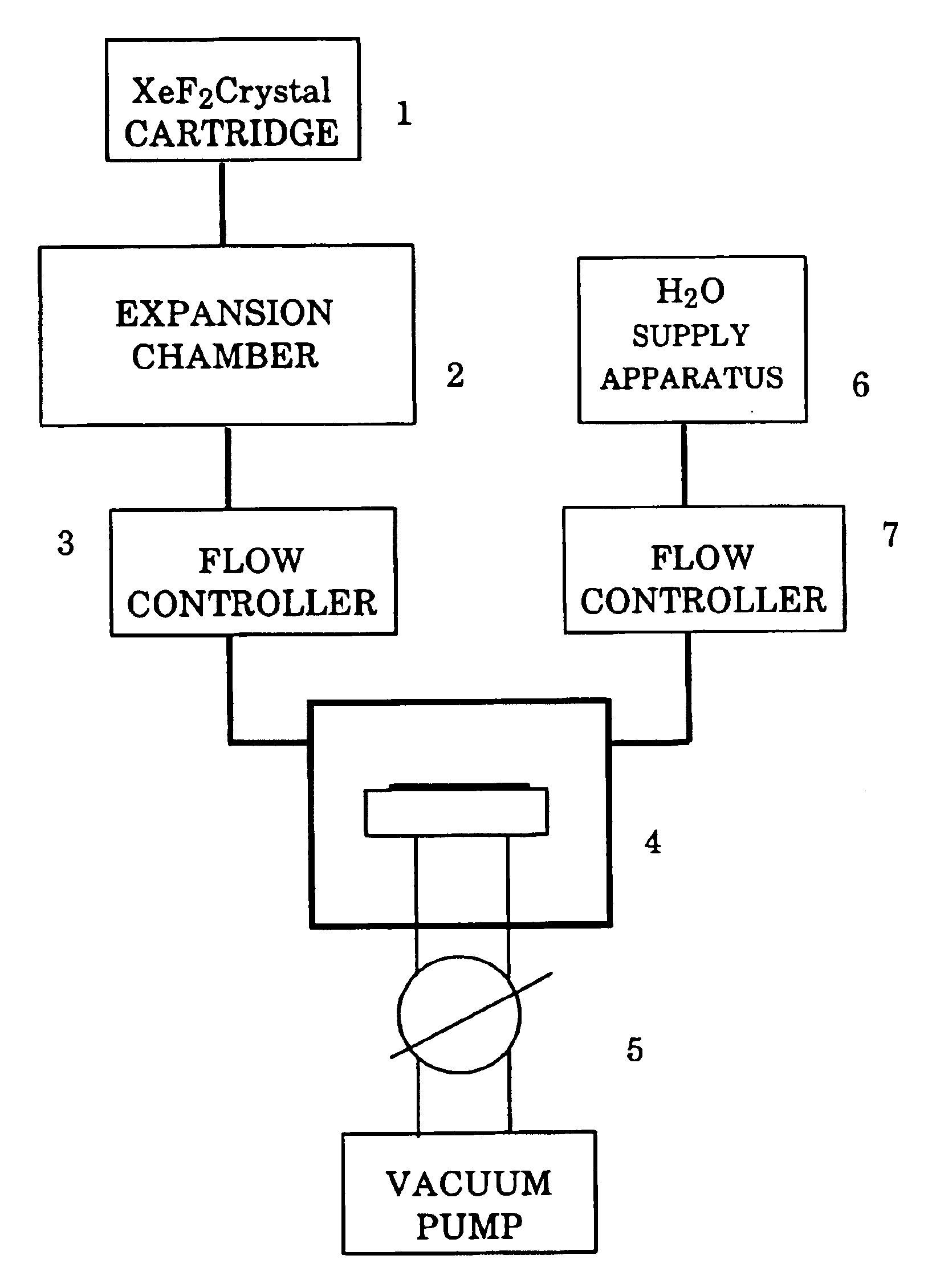
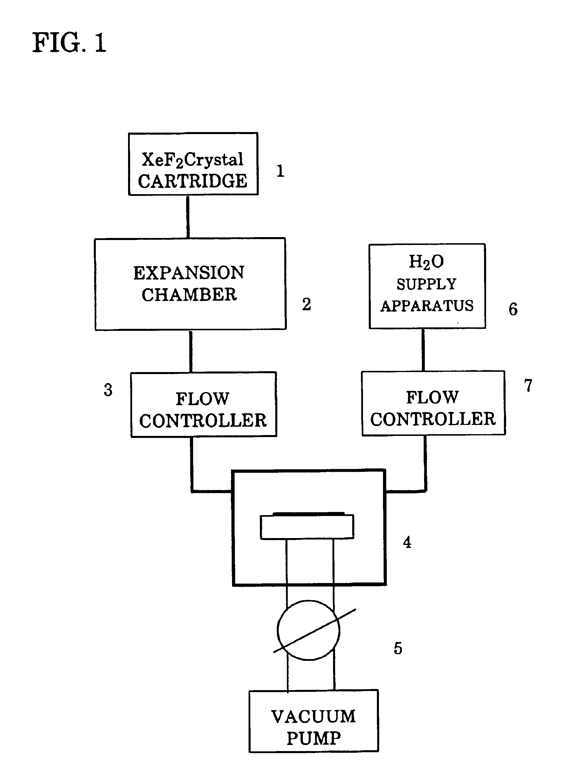
[0036]An XeF2 gas continuous supply apparatus was connected to a chamber of a publicly-known device manufacturing apparatus as shown in FIG. 1. Specifically, the continuous supply apparatus was constituted by connecting an XeF2 crystal cartridge 1 to an expansion chamber 2, and then connecting via a flow controller 3 to a pre-existing gas supply pipe leading to a process chamber 4.

[0037]In addition to a process gas supply pipe, not shown in the drawing, a vacuum pump apparatus 5 was connected to the process chamber 4, whereby the atmosphere in the chamber 4 could be controlled as desired. Consequently, it becomes possible to accurately control the flow rate of the XeF2 gas introduced into the process chamber 4, and moreover it becomes possible to control the gas flow rate and the process chamber 4 pressure independently of one another.

[0038]The inside of the process chamber 4 is evacuated from an air atmosphere to a vacuum, with a required amount of residual water being left behind ...

example 2

[0044]Using a process chamber having an XeF2 gas continuous supply apparatus as used in Example 1, etching of monocrystalline silicon wafers for devices was carried out. Note that, although not shown in the drawing, in the example of the apparatus in FIG. 1, the XeF2 gas supply port was disposed close to a stage on which the silicon wafer was placed, and a constitution preferable for an etching apparatus was adopted such that the XeF2 gas would flow uniformly over the wafer surface.

[0045]Here, 3 μm-deep pattern formation with 100 mm spacing was carried out on a 4-inch wafer. The XeF2 etching process conditions were XeF2 gas, 15 sccm, and a pressure of 20 Pa (150 mTorr).

[0046]Evacuation was carried out to create a prescribed atmosphere, and before commencing the etching, H2O was added for 5 seconds at a flow rate of 50 sccm from a separate gas introduction port without carrying out exhaustion, thus introducing water vapor into the process chamber. Then, the XeF2 gas was introduced in...

example 3

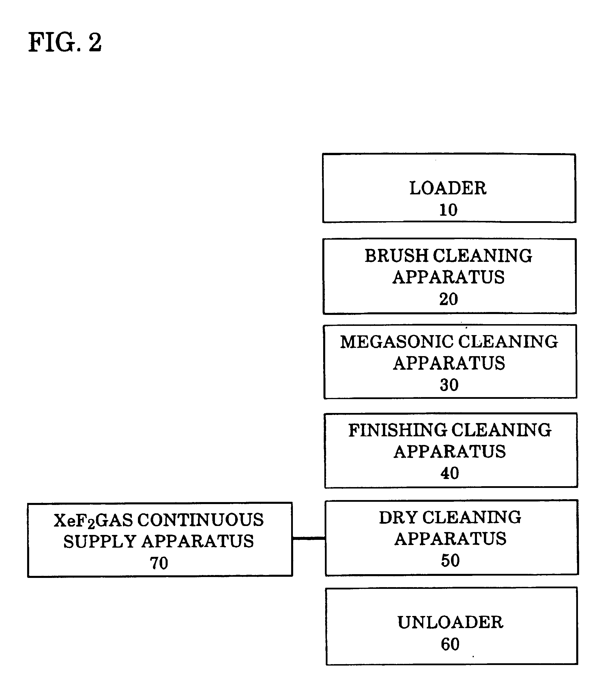
[0051]As shown in FIG. 2, a wafer carrier automatic cleaning apparatus according to the present invention has a constitution in which a loader 10, a brush cleaning apparatus 20, an ultrasonic cleaning apparatus 30, a finishing cleaning apparatus 40, a dry cleaning apparatus 50, and an unloader 60 are arranged in tandem.

[0052]A wafer carrier to be cleaned is conveyed into the cleaning apparatuses by the loader 10. The wafer carrier that has been conveyed in is then carried to the brush cleaning apparatus 20 by a robot. The brush cleaning apparatus 20 has a cleaning bath and a cleaning robot attached thereto. A cleaning liquid comprising, for example, a mixture of pure water and a neutral detergent is introduced in from a bottom part of the cleaning bath and overflows, whereby the liquid level is kept constant. The constitution is such that a rotating table is provided in the bottom part of the cleaning bath, and the carrier to be cleaned is supported in the bath in a state immersed i...


PUM

PropertyMeasurementUnit
pressureaaaaaaaaaa
pressureaaaaaaaaaa
timeaaaaaaaaaa

Abstract

A cleaning method for removing fats, oils, and silicon small particles, which are conventionally difficult to remove, adhering to devices and carriers used to manufacture a semiconductor wafer or a semiconductor device. An etching method is also disclosed. XeF2 gas produced by sublimation is made to contact with an object to be cleaned in a vacuum atmosphere so as to decompose and gasify the oils and fats and to remove silicon small particles by etching. Prior to the cleaning, when a trace amount of residual water is left in the vacuum atmosphere, H2O reacts with XeF2, and HF is produced. For example, a native oxide SiO2 formed on the surface of silicon small particles can be removed, and XeF2 directly reacts with silicon, therby enabling etching. The cleaning etching rates are extremely high.

Description

[0001]This is a U.S. national phase application under 35 U.S.C. §371 of International Patent Application No. PCT / JP01 / 11059, filed Dec. 17, 2001, and claims the benefit of International Patent Application No. PCT / JP00 / 08974 filed Dec. 18, 2000. The International Application was published in Japanese on Jun. 27, 2002 as WO 02 / 50884 A1, under PCT Article 21(2).TECHNICAL FIELD[0002]The present invention relates to, in a semiconductor wafer or semiconductor device manufacturing process, methods and apparatuses for removing by cleaning dust from a silicon wafer, extremely minute silicon pieces that have become stuck in a carrier, or an oil film or the like caused by oily components or the like that have leaked out from a pump or the like of any of various manufacturing apparatuses installed in a clean room or sebum generated from workers, and more specifically relates to a dry cleaning method, an etching method, and apparatuses therefor that enable the removal of polymer, grease, metal, ...

Claims


Application Information

Patent Timeline
Patent Type & Authority Patents(United States)
IPC IPC(8): B08B5/00C03C23/00C23G1/00C23F1/00G01L21/00G01L21/30G01R31/00H01L21/02H01L21/304H01L21/306H01L21/3065B01D11/04C10G21/18
CPCA23K1/146B01D11/0488H01L21/02046H01L21/02049H01L21/3065A23K10/37Y02P60/87
Inventor KANAYAMA, TOKIKOKOUNO, HIROAKI
Owner SUMITOMO PRECISION PROD CO LTD
Why Eureka
Try Eureka