Electron-emitting device having carbon films with a particular orientation, electron source using electron-emitting device, and image forming apparatus
a carbon film, electron-emitting technology, applied in the direction of electric discharge tube/lamp manufacture, discharge tube luminescnet screen, discharge tube with screen, etc., can solve the problems of unstable or deteriorated electron emission characteristics, chemical changes, and rapid deterioration of electron emission characteristics, etc., to achieve excellent uniformity and stability, excellent efficiency, and excellent uniformity
- Summary
- Abstract
- Description
- Claims
- Application Information
AI Technical Summary
Benefits of technology
Problems solved by technology
Method used
Image
Examples
example 1
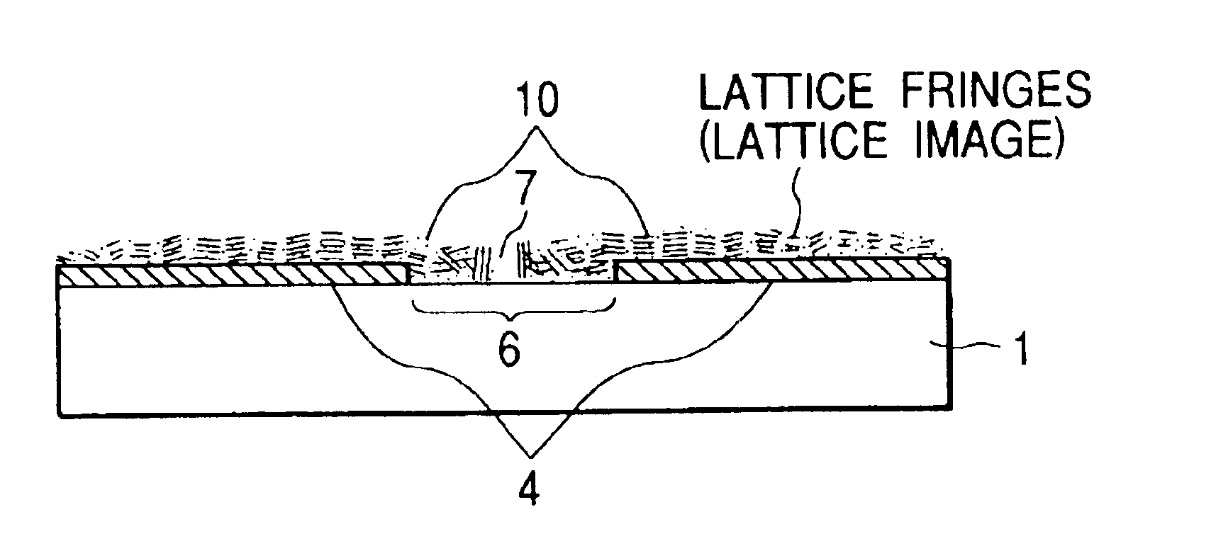
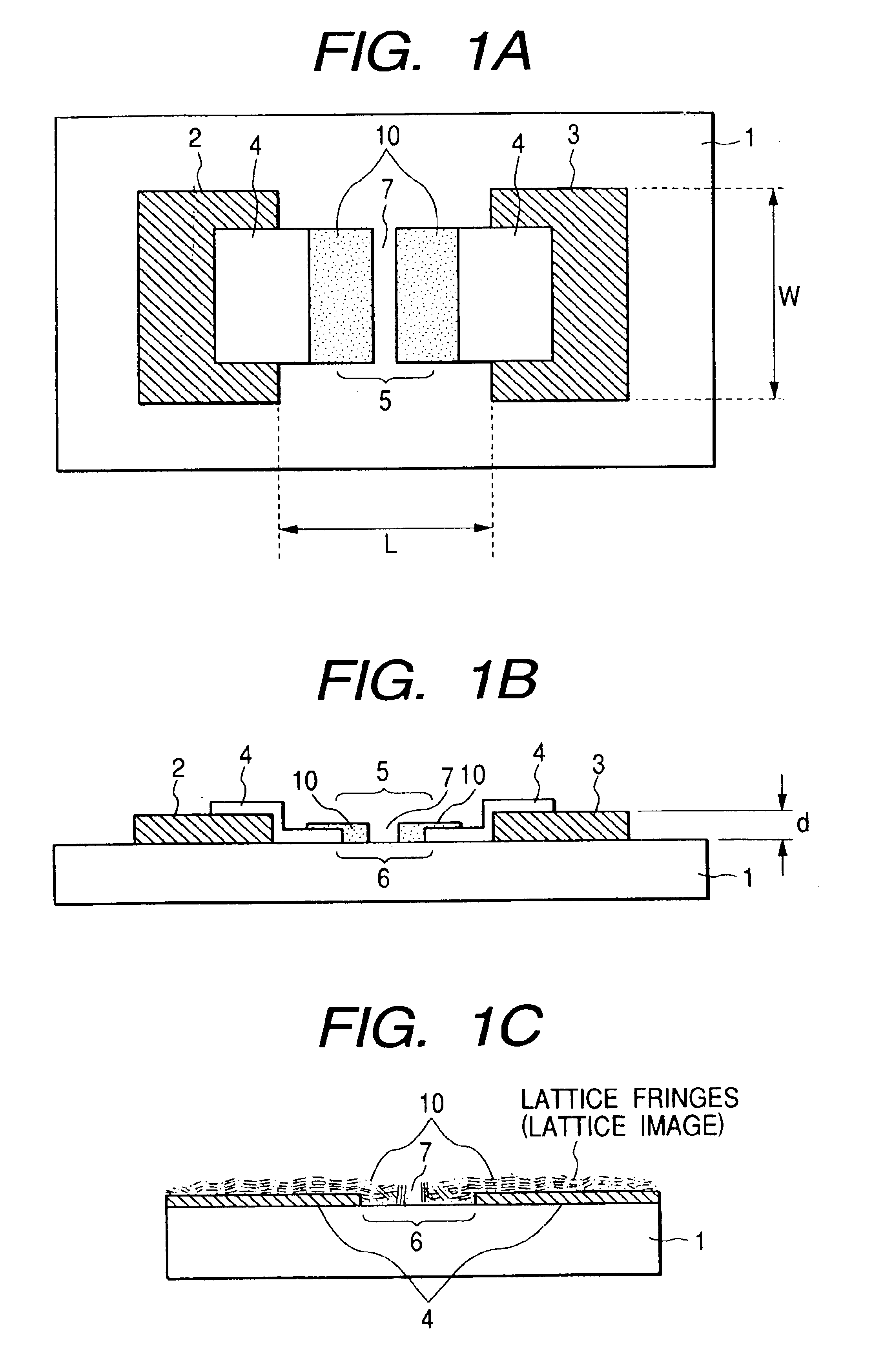
[0155]The electron-emitting device formed by the present example is configured as schematically shown in FIGS. 1A and 1B.
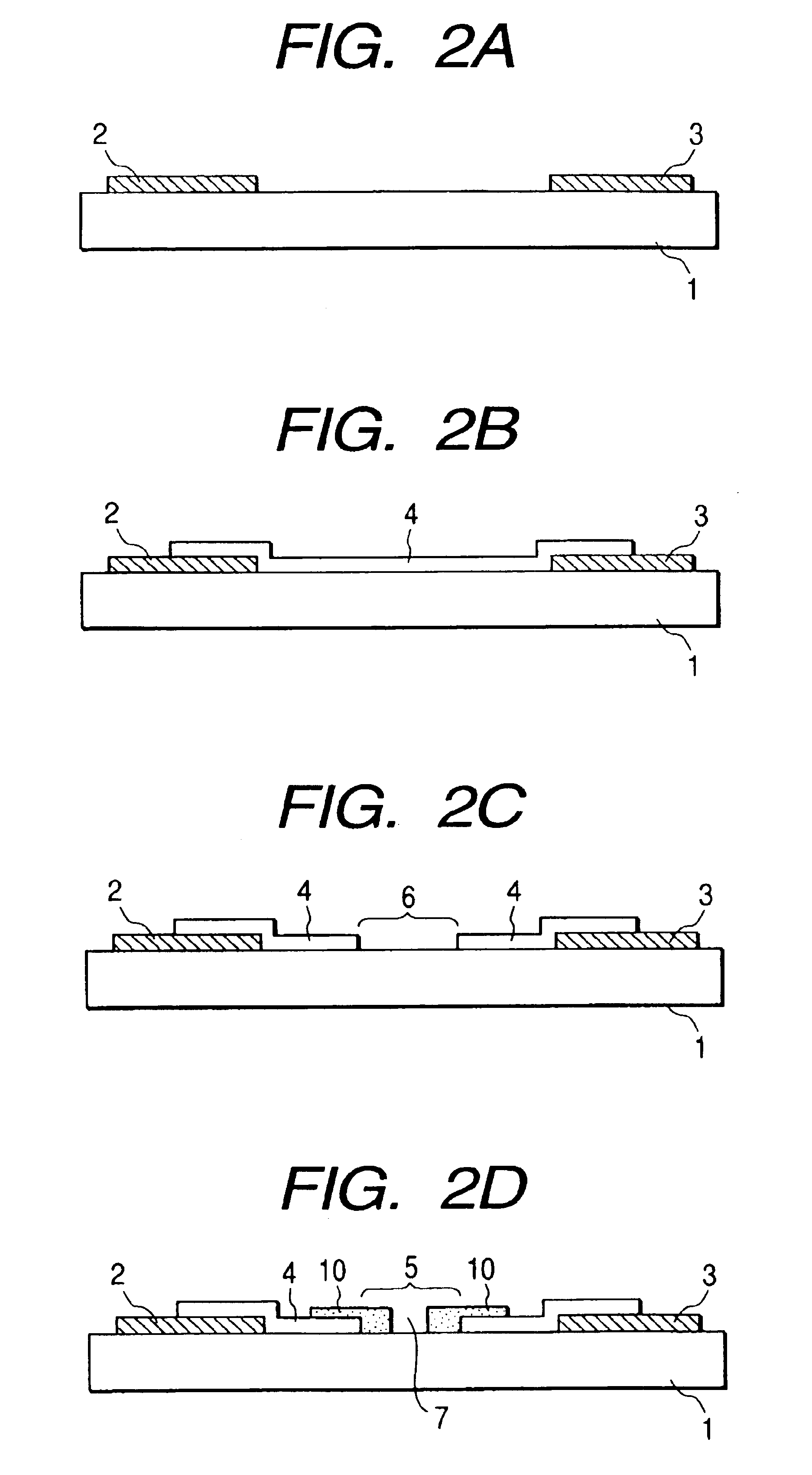
[0156]The manufacturing steps of the electron-emitting device produced in the present example are described using drawings as follows.
[0157]Step-a
[0158]Quartz has been used as the substrate 1, and after cleaning this with detergent, pure water, and organic solvent, the photoresist RD-2000N (produced by Hitachi Chemical Co., Ltd.) has been applied with spinner (2500 rpm for 40 seconds), and pre-baking has been implemented at 80° C. for 25 minutes.
[0159]Next, using a mask corresponding to the device electrode pattern, contact exposure has been implemented, and developing using developer has been implemented, and post-baking at 120° C. for 20 minutes has been implemented and thus the resist mask has been formed.
[0160]Next, Ni has been film-formed with the vacuum evaporation method. The film-forming rate has been 0.3 mm / second with film thickness being 10 nm.
[0161]Nex...
example 2
[0178]The present example is a manufacturing method of the electron source of the matrix wiring schematically shown in FIG. 14, and of the image forming apparatus (FIG. 9) using this electron source. FIG. 14 is a partial plan view showing as a schematic diagram the configuration of the electron source of the matrix wiring formed by the present example, and the sectional configuration along a polygonal line 15—15 in FIG. 14 is shown in FIG. 15. With reference to FIGS. 16A to 16D and FIGS. 17E to 17G, the manufacturing step of the electron source is described, and moreover the manufacturing step of the image forming apparatus is also described as follows.
[0179]Step-A
[0180]Silicon oxide film of 0.5 μm has been formed by sputtering method on a blue plate glass which has been cleaned, and the product is treated as the substrate 1, and Cr 5 nm and Au 600 nm have been film-formed thereon by vacuum evaporation method in succession, thereafter, the photoresist AZ1370 (produced by Hoechst Cor...
example 3
[0203]The electron-emitting device has been formed in steps similar to those in the example 1 except that the step-d of the example 1 has been changed to the step-D2 as shown below.
[0204]Step-D2
[0205]Next, the gas inside the vacuum chamber 35 has been evacuated by the evacuation apparatus 36, and after the pressure reach not more than 1.3×10⁻⁵ Pa, acrylonitrile has been introduced and the pressure has been set at 1.3×10⁻³ Pa. At first, the rectangular wave pulses which invert polarity while gradually increasing the wave height value as shown in FIG. 13B have been repeatedly applied to between the device electrodes. Here, the pulse width T3 has been set at 1 msec. and the pulse interval T4 has been set at 10 msec., and the wave height value has been gradually increased from 10 V to 15 V over 35 minutes. At that time, when the pulse voltage has not been applied to between the device electrodes, an electron beam has been radiated as pulses to the devices from the electron gun (not show...
PUM
 Abstract
Description
Claims
Application Information


