
High thermal performance packaging for optoelectronics devices

a technology of optoelectronics and thermal performance, applied in the direction of ion implantation coating, printed circuit aspects, electric discharge heating, etc., can solve the problems of high junction temperature, local heating effect, high power density generated inside the material, etc., to achieve maximum efficiency, high power injection, and the effect of long li

Inactive Publication Date: 2015-03-24
PHOTONSTAR LED
View PDF18 Cites 0 Cited by
  • Summary
  • Abstract
  • Description
  • Claims
  • Application Information

AI Technical Summary

Benefits of technology

The present invention allows for continuous high power injection into a small device while keeping it cool and efficient. This is achieved through a light emitting module that allows for fast heat conduction and isolation between the electrical pathways needed to drive the device. The result is longer lifetimes for the device and optimal performance.

Problems solved by technology

This is due to the inherent conflict between thermal conductivity and electrical insulation when selecting suitable materials for packaging.
The largest challenges associated with the packaging come from electrically pumped light emitting devices.
These comprise of a chip level small format device and are typically driven at high drive currents resulting in high power densities generated inside the material causing local heating effects.
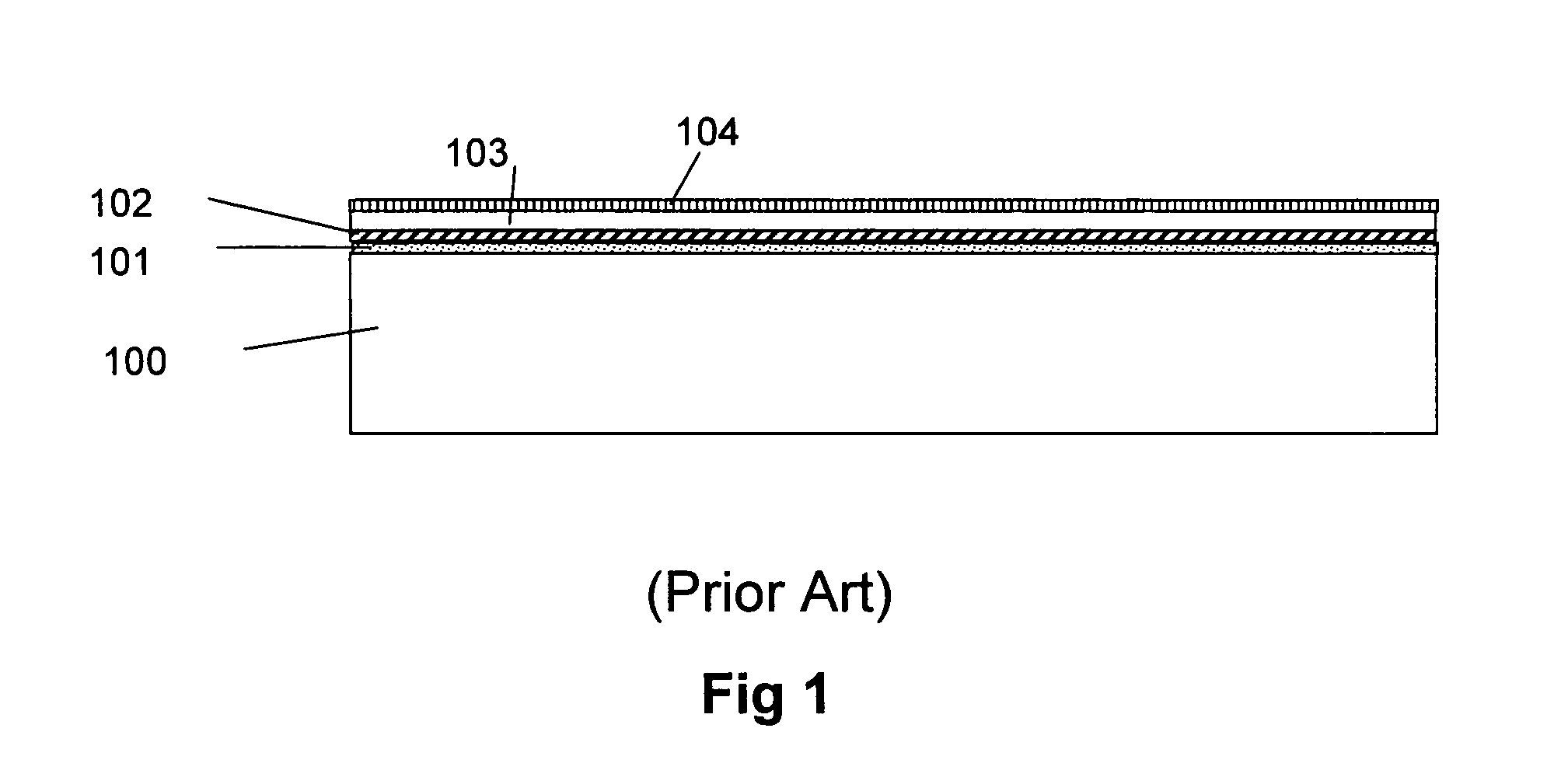
However if this type of IMS-PCB is used with the LED placed directly on the PCB then high junction temperatures will occur as the thermal load will not be able to spread adequately in layer 103.
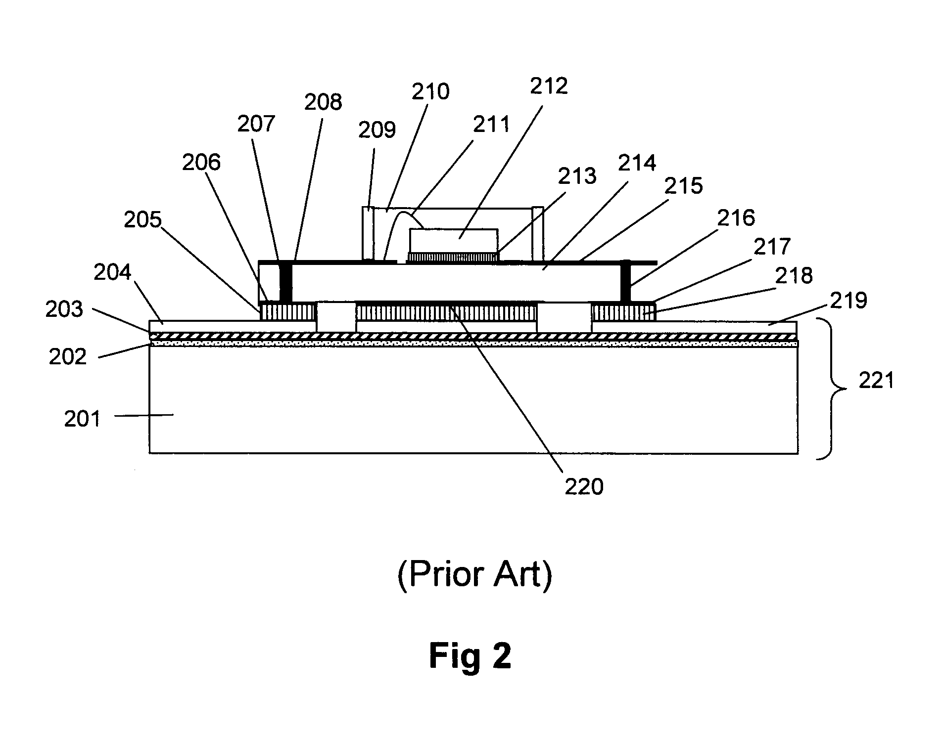
Of course, all these layers of packaging create extra cost and extra interfaces that increase thermal resistance.
This is an important issue if typical metal, graphite or conductive plastic heat sinks are used to prevent the heat sink becoming electrically live.

Method used


Image

  • High thermal performance packaging for optoelectronics devices
  • High thermal performance packaging for optoelectronics devices
  • High thermal performance packaging for optoelectronics devices

Examples


Embodiment Construction

[0051]The thermal conductivity of a material can be defined as follows:

[0052]k=Qt×LA×Δ⁢⁢T(1)

where Q is the quantity of heat transmitted in time t through a thickness L in a direction normal to a surface of area A, due to a temperature difference ΔT, under steady state conditions and when the heat transfer is dependent only on the temperature gradient.

[0053]In order to reduce the temperature difference across a defined region in a submount a material with a higher thermal conductivity can be employed, additionally a thinner material may also be implemented. However, care has to taken that reducing the thickness still maintains good electrical insulation and maintains high electrical breakdown voltages. Table 1 contains a list of thermal conductivities for common materials used in semiconductors, light emitting devices, and LED packaging.

[0054]

TABLE 1ThermalConductivityCTE (10−6 / K)MaterialW / (m · K)@ 20° C.Alumina186.9Aluminum Nitride1704.7AuSn solder5716Copper40017Aluminium23724Tungst...


PUM

PropertyMeasurementUnit
thermal conductivityaaaaaaaaaa
electrical breakdown voltageaaaaaaaaaa
thicknessaaaaaaaaaa

Abstract

A novel submount for the efficient dissipation of heat away from a semiconductor light emitting device is described, which also maintains efficient electrical conductivity to the n and p contacts of the device by separating the thermal and electrical conductivity paths. The submount comprises at least the following constituent layers: a substrate (400) with thermally conductive properties; a deposited layer (402) having electrically insulating and thermally conducting properties disposed on at least a region of the substrate having a thickness of between 50 nm and 50 microns; a patterned electrically conductive circuit layer (404) disposed on at least a region of the deposited layer; and, a passivation layer at least partially overcoating a top surface of the submount. Also described is a light emitting module employing the substrate and a method of manufacture of the submount.

Description

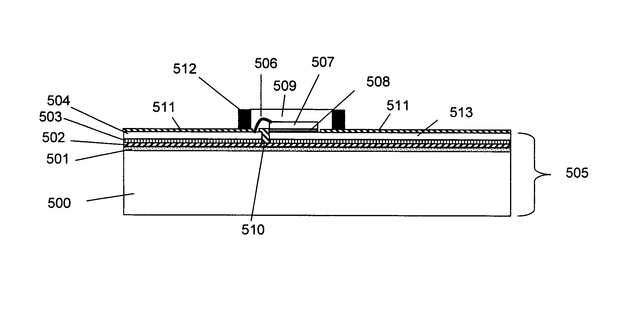
[0001]This application is a national phase of International Application No. PCT / GB2008 / 002873 filed Aug. 22, 2008, and published in the English language as WO 2009 / 024801 on Feb. 26, 2009.FIELD OF THE INVENTION[0002]The present invention relates to an improved packaging approach for Light Emitting Diode (LED) devices.BACKGROUND TO THE INVENTION[0003]There are many types of packages used to manage the thermal, optical and electrical connections to small optoelectronic devices. This is due to the inherent conflict between thermal conductivity and electrical insulation when selecting suitable materials for packaging. Typical Optoelectronic devices include lasers, LEDs, detectors and photovoltaic devices. The largest challenges associated with the packaging come from electrically pumped light emitting devices. The associated wall plug efficiency of the device dictates that the conversion from electrical energy to photons out is never unity thereby introducing substantial heating in the ...

Claims


Application Information

Patent Timeline
Patent Type & Authority Patents(United States)
IPC IPC(8): H01L29/72H01L33/64H05K1/05H05K3/38
CPCH05K1/053H01L33/641H05K3/388H05K2201/0179H05K2201/10106H01L2224/32225H01L2224/48091H01L2224/48227H01L2224/73265H01L2924/19107H01L2924/00014H01L2924/00H01L33/64H01S5/00
Inventor MCKENZIE, JAMES STUARTZOOROB, MAJD
Owner PHOTONSTAR LED
Learn More