High-work-efficiency multilayered circuit board

a multi-layer circuit board, high-work-efficiency technology, applied in the direction of multiple-port network, inductance, association of printed circuit non-printed electric components, etc., can solve the problems of large number of components, increase cost and thickness, and reduce production efficiency, and achieve low parts count and high work efficiency

Inactive Publication Date: 2005-07-26
ALPS ALPINE CO LTD
View PDF6 Cites 6 Cited by
  • Summary
  • Abstract
  • Description
  • Claims
  • Application Information

AI Technical Summary

Benefits of technology

[0020]Accordingly, it is an object of the present invention to provide an inexpensive thin multilayered circuit board with low parts count and high work efficiency.

Problems solved by technology

The known multilayered circuit boards including the inductor and the capacitor require at least three insulating layers, thus disadvantageously including a large number of components to increase the cost and the thickness.
The use of three insulating layers poses the problems of requiring much time and labor for production and needing through-hole conduction work in at least one part, thus decreasing production efficiency.

Method used


Image

  • High-work-efficiency multilayered circuit board
  • High-work-efficiency multilayered circuit board
  • High-work-efficiency multilayered circuit board

Examples


first embodiment

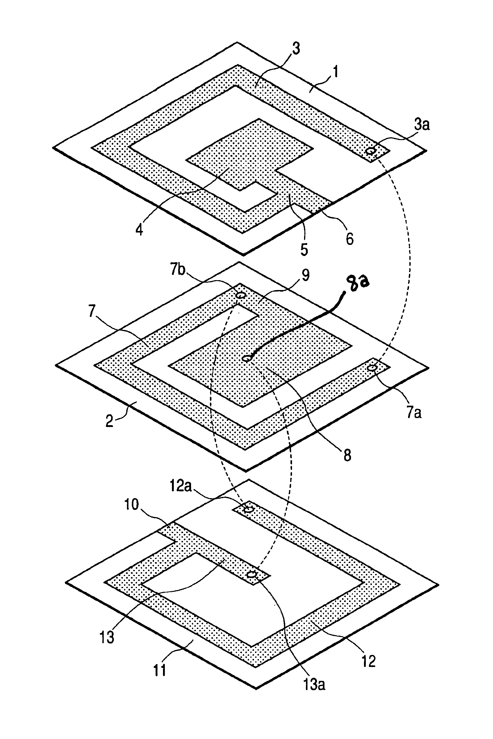
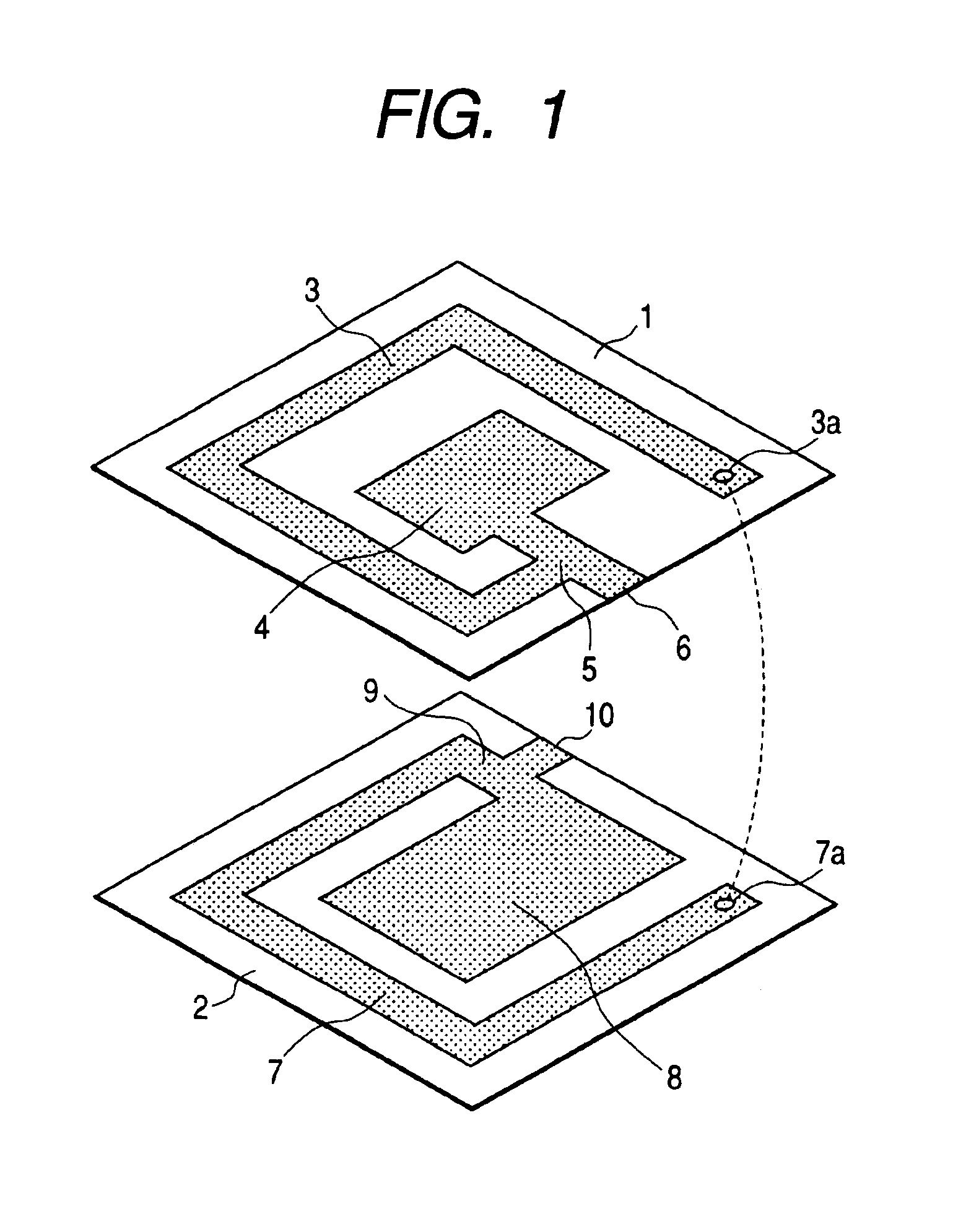
[0041]Referring first to FIG. 1, the arrangement of a multilayered circuit board will be described in which an inductor and a capacitor are connected in parallel. First and second insulating layers 1 and 2 made of ceramic such as low-temperature co-fired ceramic (LTCC) are stacked in order to form a multilayered ceramic substrate (low-temperature co-fired ceramic substrate).

[0042]The first insulating layer 1 has on its surface a first U-shaped electric conductor 3 formed of a conductive film of silver or the like and provided along the outer periphery of the first insulating layer 1, a first rectangular electrode 4 provided inside the first electric conductor 3 and in the center of the first insulating layer 1, a first connecting conductor 5 that connects the first electric conductor 3 and the first electrode 4, and a first extension 6 provided to the first connecting conductor 5.

[0043]The second insulating layer 2 has on its surface a second U-shaped electric conductor 7 formed of...

second embodiment

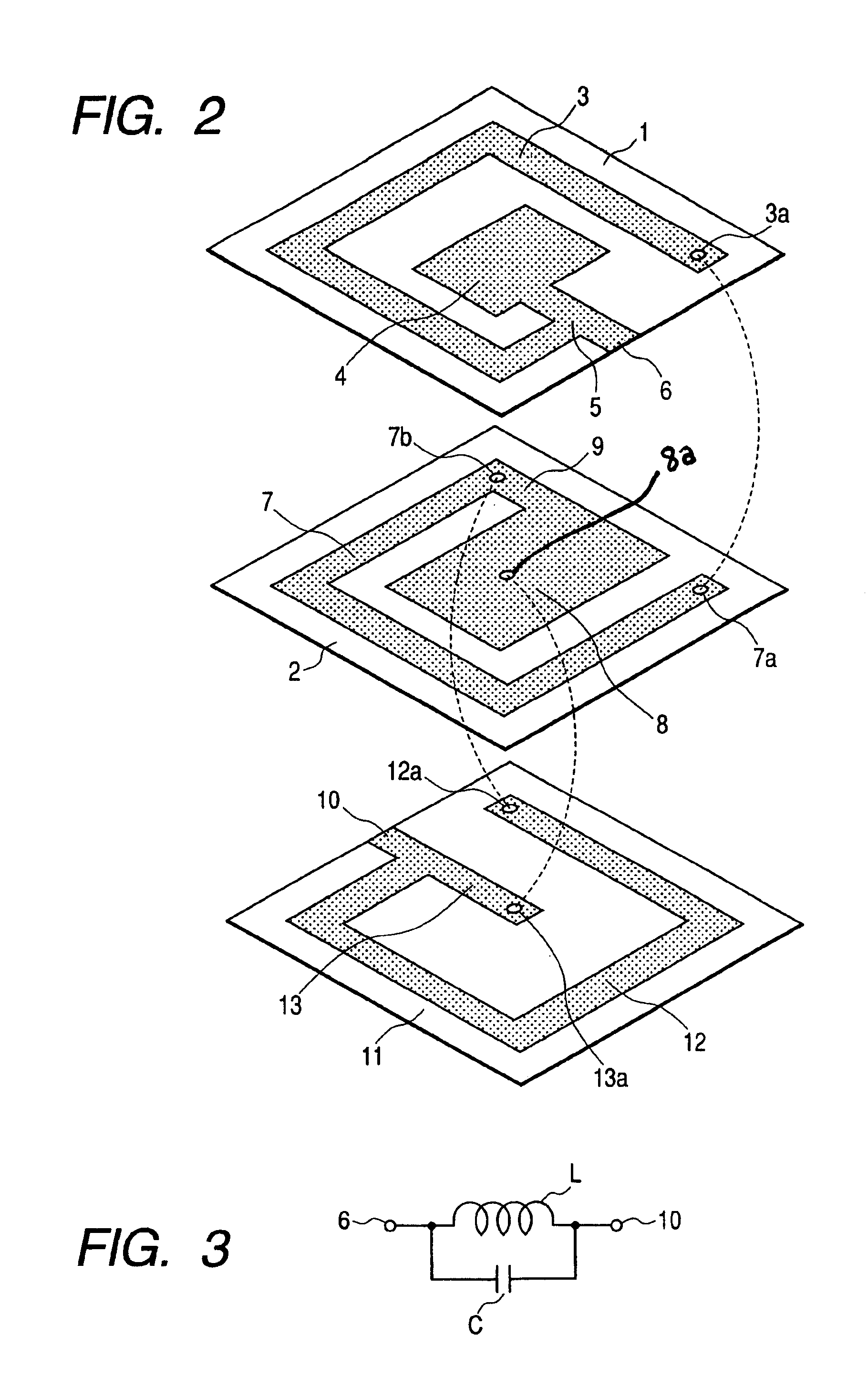
[0048]Referring next to FIG. 2, the arrangement of a multilayered circuit board will be described in which an inductor and a capacitor are connected in parallel. First, second, and third insulating layers 1, 2, and 11 made of ceramic such as LTCC are stacked in layers to form a multilayered ceramic substrate (low-temperature co-fired ceramic substrate).

[0049]The first insulating layer 1 has on its surface the first U-shaped electric conductor 3 formed of a conductive film of silver or the like and provided along the outer periphery of the first insulating layer 1, the first rectangular electrode 4 provided inside the first electric conductor 3 and in the center of the first insulating layer 1, the first connecting conductor 5 that is made of a conductive film of silver or the like and connects the first electric conductor 3 and the first electrode 4, and the first extension 6 provided to the first connecting conductor 5.

[0050]The second insulating layer 2 has on its surface the sec...

third embodiment

[0058]Referring now to FIG. 4, the arrangement of a multilayered circuit board will be described in which an inductor and a capacitor are connected in series. First and second insulating layers 21 and 22 made of ceramic such as LTCC are stacked in order to form a multilayered ceramic substrate (low-temperature co-fired ceramic substrate).

[0059]The first insulating layer 21 has on its surface a first U-shaped electric conductor 23 formed of a conductive film of silver or the like and provided along the outer periphery of the first insulating layer 21, a first rectangular electrode 24 provided inside the first electric conductor 23 and in the center of the first insulating layer 21, a first connecting conductor 25 formed of a conductive film of silver or the like and connecting the first electric conductor 23 and the first electrode 24, and a first extension 26 provided at the end of the first electric conductor 23.

[0060]The second insulating layer 22 has on its surface a second rect...


PUM

PropertyMeasurementUnit
electricaaaaaaaaaa
conductiveaaaaaaaaaa
electric conductoraaaaaaaaaa

Abstract

A multilayered circuit board according to the present invention includes at least first and second stacked insulating layers. The first insulating layer has thereon a first electric conductor made of a conductive film constituting an inductor and a first electrode made of a conductive film constituting a capacitor. The second insulating layer has thereon a second electrode made of a conductive film constituting a capacitor. The first and second insulating layers are stacked such that the first and second electrodes are opposed to each other through the insulating layers. Therefore this provides a circuit board having a capacitor and an inductor through the use of the two insulating layers, thus providing an inexpensive thin circuit board with small parts count and high work-efficiency compared with the use of three insulating layers in a related art.

Description

BACKGROUND OF THE INVENTION[0001]1. Field of the Invention[0002]The present invention relates to a multilayered circuit board suitable for use in an electric circuit of a band-pass filter or the like.[0003]2. Description of the Related Art[0004]Known multilayered circuit boards will be described. FIG. 8 is an exploded perspective view of a known multilayered circuit board in which an inductor and a capacitor are connected in parallel; FIG. 9 is a circuit diagram of the multilayered circuit board of FIG. 8; FIG. 10 is an exploded perspective view of a known multilayered circuit board in which an inductor and a capacitor are connected in series; and FIG. 11 is a circuit diagram of the multilayered circuit board of FIG. 10.[0005]Referring to FIG. 8, the arrangement of the multilayered circuit board in which an inductor and a capacitor are connected in parallel will be described. First, second, and third ceramic insulating layers 51, 52, and 53 are stacked on top of each other in layers...

Claims


Application Information

Patent Timeline
Patent Type & Authority Patents(United States)
IPC IPC(8): H01F17/00H03H7/01
CPCH01F17/0013H03H7/0115H01F2017/0026H03H2001/0085
Inventor AOYAGI, TORU
Owner ALPS ALPINE CO LTD
Why Eureka
Try Eureka