Data strobe synchronization circuit and method for double data rate, multi-bit writes

a data strobe and data synchronization technology, applied in the field of memory devices, can solve the problems of incorrect write data being strobed into the memory device, noise on the ds line, and misinterpreting the ds pulse as a ds puls

Inactive Publication Date: 2005-07-26
MICRON TECH INC
View PDF18 Cites 39 Cited by
  • Summary
  • Abstract
  • Description
  • Claims
  • Application Information

AI Technical Summary

Problems solved by technology

One problem that may exist with DDR2 memory devices is that noise on the DS line in a “preamble” prior to the first DS pulse may be misinterpreted as a DS pulse, particularly where the DS pulse is substantially delayed relative to the data.
Under these circumstances, the incorrect write data may be strobed into the memory device.

Method used


Image

  • Data strobe synchronization circuit and method for double data rate, multi-bit writes
  • Data strobe synchronization circuit and method for double data rate, multi-bit writes
  • Data strobe synchronization circuit and method for double data rate, multi-bit writes

Examples


Embodiment Construction

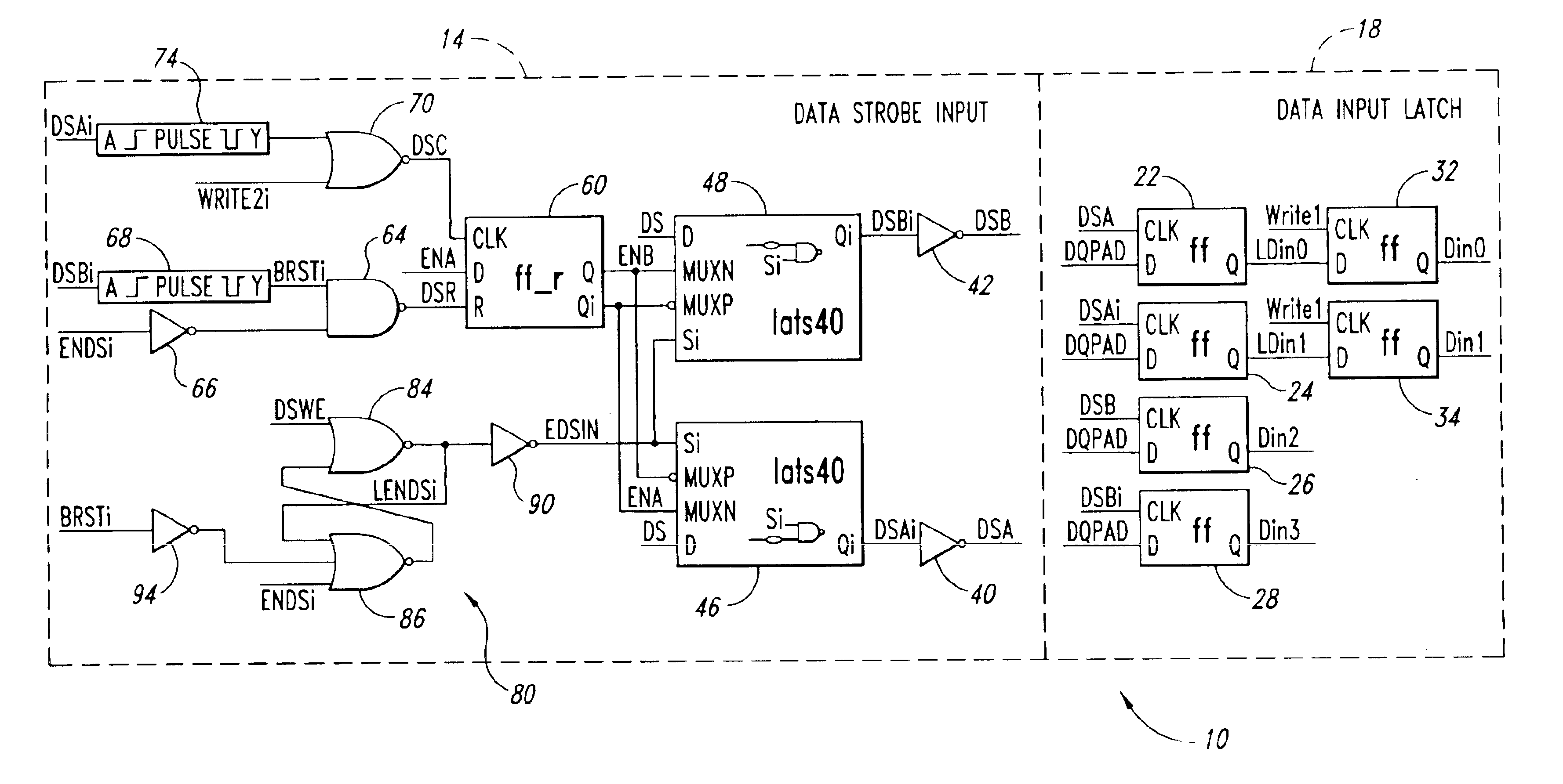
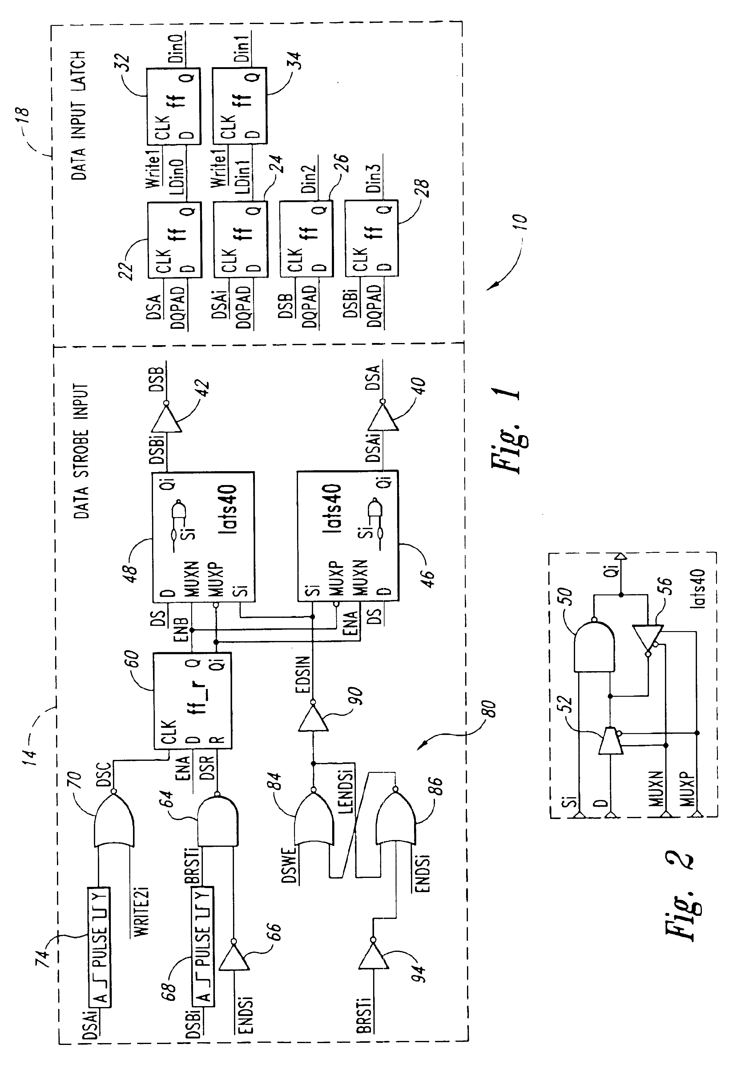
[0014]One embodiment of a data strobe circuit 10 that is insensitive to noise on data strobe lines and thus captures write data responsive only to valid data strobes is shown in FIG. 1. As explained more fully below, the circuit 10 operates by strobing data on each transition of a DS pulse on a data strobe DS line, saving the data strobed on the last two transitions prior to a predetermined write command, and saving the data strobed on the first two transitions following the predetermined write command. As a result, any data strobed by noise signals in the preamble are overwritten with correctly strobed data.

[0015]With reference to FIG. 1, the data strobe circuit 10 includes a data strobe input circuit 14 and a data input latch circuit 18. As described in greater detail below, the data strobe input circuit 14 functions to generate data strobe signals, and the data input latch circuit 18 uses those strobe signals to latch four bits of write data.

[0016]The data input latch circuit 18 ...


PUM


Abstract

A data strobe synchronization circuit includes first and second logic circuits receiving global data strobe pulses and respective enable signal. A control circuit initially applies an enable signal to the first logic circuit so that the first logic circuit generates a first data strobe pulse responsive to each global data strobe pulse. The control circuit receives a write control signal. When the write control signal becomes active, the control circuit terminates the enable signal applied to the first logic circuit and applies an enable signal to the second logic circuit. The second logic circuit then generates a second data strobe pulse responsive to the next global data strobe pulse. The first and second data strobe pulses are used to latch a data signal in respective flip-flops. The data strobe pulses may latch the data signal in pairs of flip-flops on the leading and trailing edges of the data strobe pulses.

Description

TECHNICAL FIELD[0001]This invention relates to memory devices, and, more particularly to a circuit and method for strobing multiple bits of write data into a double data rate memory device.BACKGROUND OF THE INVENTION[0002]Memory devices, such as dynamic random access memory (“DRAM”) devices, are commonly used in a wide variety of applications, including personal computers. A great deal of effort has been devoted, and is continuing to be devoted, to increasing the speed at which memory devices are able to read and write data. Initially, memory devices operated asynchronously, and a single set of data were read from or written to the memory device responsive to a set of memory commands. The data bandwidth of memory devices were subsequently increased by reading and writing data in synchronism with a clock signal. Synchronously reading and writing data also allowed for other advances in the data bandwidth of memory devices, such as burst mode and page mode DRAMs, in which a large amoun...

Claims


Application Information

Patent Timeline
Patent Type & Authority Patents(United States)
IPC IPC(8): G11C7/10G11C7/22G11C8/00G11C11/4076G11C11/4094
CPCG11C7/1066G11C7/1078G11C7/1087G11C7/1093G11C7/22G11C11/4076G11C11/4094G11C7/10G06F3/06
Inventor MORZANO, CHRISTOPHER K.LI, WEN
Owner MICRON TECH INC
Why Eureka
Try Eureka