Configurable high-speed memory interface subsystem

a memory interface and high-speed technology, applied in the field of memory interfaces, can solve the problems of re-using the physical interface, the inflexibility of conventional approaches to apply a particular physical interface ip,

Inactive Publication Date: 2008-10-14
BROADCOM INT PTE LTD
View PDF5 Cites 36 Cited by
  • Summary
  • Abstract
  • Description
  • Claims
  • Application Information

AI Technical Summary

Benefits of technology

[0006]The objects, features and advantages of the present invention include providing a configurable high-speed memory interface subsystem that may (i) provide compile time configurable bus widths of the physical interface IP, (ii) provide complete physical interfaces for DDR2 / DDR1 SDRAM memory applications, (iii) provide automatic data alignment of receive data over PVT using synchronous read FIFOs, (iv) provide automatic one-quarter or one-fifth cycle clock forwarding over PVT on the receive data path, (v) provide in phase data transfer (transmit and receive) to enable implementation of proprietary chip-to-chip DDR interfaces, (vi) support upper level system software functions (e.g., read data strobe Gating and read data strobe centering techniques) for DDR2 / DDR1 SDRAM memory applications, (vii) control automatic impedance update function for the IO buffers, (viii) provide reusable IP in a variety of DDR applications (e.g., DDR1, DDR2, or chip-to-chip proprietary DDR interfaces), (ix) provide IP that supports different bus configurations or different system bus topologies, (x) enable easy product implementation, (xi) provide a migration path by providing similar physical interfaces to upper level memory controller function and / or (xii) provide a subsystem function that encapsulates all low-level physical data transfer and IO buffer housekeeping functions for the DDR2 / DDR1 / proprietary DDR interfaces.

Problems solved by technology

The conventional approaches do not have the flexibility to apply a particular physical interface IP for different DDR SDRAM memory bus configurations.
The conventional approaches restrict the re-use of the physical interface IP in applications that have different system topologies.

Method used


Image

  • Configurable high-speed memory interface subsystem
  • Configurable high-speed memory interface subsystem
  • Configurable high-speed memory interface subsystem

Examples


Embodiment Construction

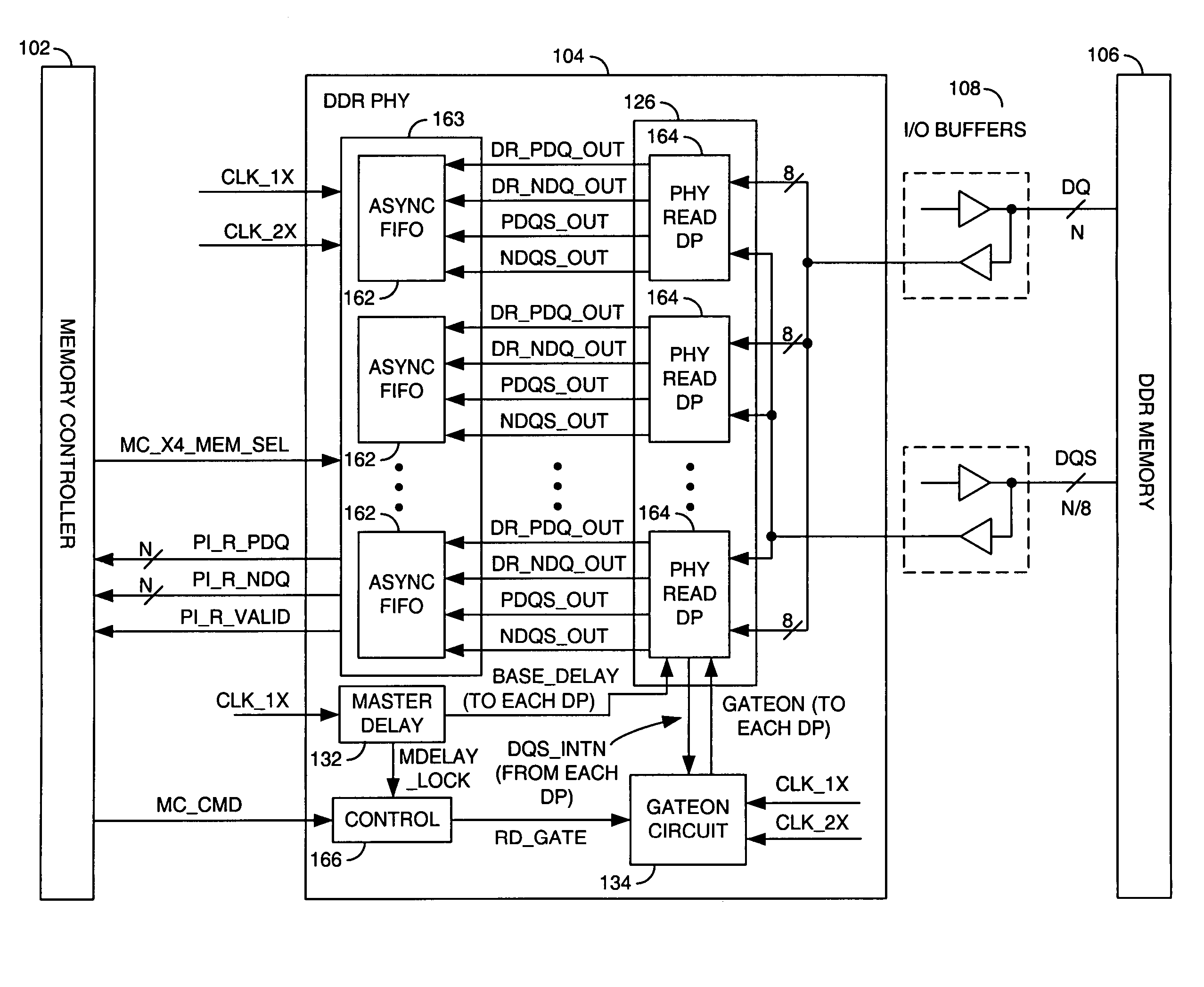
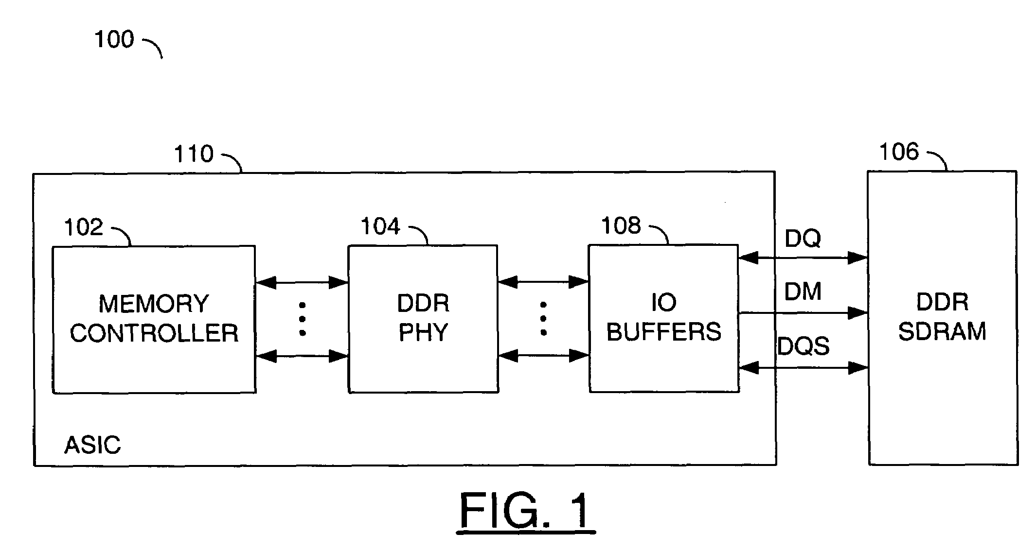
[0017]Referring to FIG. 1, a block diagram is shown illustrating a system 100 in which one or more preferred embodiments of the present invention may be implemented. In one example, the system 100 may comprise a circuit (or block) 102, a circuit (or block) 104, a circuit (or block) 106 and a circuit (or block) 108. The circuit 102 may be implemented as a memory controller. The circuit 104 may be implemented as a memory interface. In one example, the circuit 104 may be implemented as a double data rate (DDR) physical layer core (PHY). The circuit 106 may be implemented as one or more double data rate (DDR) synchronous dynamic random access memory (SDRAM) devices. The circuit 108 may be implemented, in one example, as stub series terminated logic (SSTL) IO buffers. In one example, the IO buffers 108 may be implemented as SSTL-2 buffers. The circuit 104 may be coupled between the circuit 102 and the circuit 106. In one example, the circuit 104 may be coupled to the circuit 106 by the c...


PUM


Abstract

A core including a write logic IP block, a read logic IP block, a master delay IP block and an address and control IP block. The write logic IP block may be configured to communicate data from a memory controller to a double data rate (DDR) synchronous dynamic random access memory (SDRAM). The read logic IP block may be configured to communicate data from the double data rate (DDR) synchronous dynamic random access memory (SDRAM) to the memory controller. The master delay IP block may be configured to generate one or more delays for the read logic IP block. The address and control logic IP block may be configured to control the write logic IP block and the read logic IP block. The core is generally configured to couple the double data rate (DDR) synchronous dynamic random access memory (SDRAM) and the memory controller.

Description

FIELD OF THE INVENTION[0001]The present invention relates to memory interfaces generally and, more particularly, to a configurable high-speed memory interface subsystem.BACKGROUND OF THE INVENTION[0002]Conventional approaches for interfacing a memory controller function with a double data rate (DDR) synchronous dynamic random access memory (SDRAM) use hard-coded intellectual property (IP) blocks for specific DDR SDRAM memory applications. For different data bus width applications, different physical interfaces are created. On the receive data path, the conventional approach is to perform a detailed SPICE (simulation program for integrated circuit emphasis) timing analysis and to carefully construct the read data path, such that the receive data can be re-synchronized to the memory controller function.[0003]The conventional approaches do not have the flexibility to apply a particular physical interface IP for different DDR SDRAM memory bus configurations. The conventional approaches ...

Claims


Application Information

Patent Timeline
Patent Type & Authority Patents(United States)
IPC IPC(8): G06F12/00
CPCG11C7/1051G11C7/1057G11C7/1066G11C7/1078G11C7/1084G11C7/1093G11C7/22G11C7/225G11C11/4076G11C11/4096G11C2207/2254
Inventor BUTT, DERRICK SAI-TANGKONG, CHENG-GANGMAGEE, TERENCE J.
Owner BROADCOM INT PTE LTD
Why Eureka
Try Eureka