Input/output cells for a double data rate (DDR) memory controller

a memory controller and input/output cell technology, applied in the field of memory devices, can solve the problems of increasing the complexity of the timing considerations for reading and writing data to and from the ddr memory, the delay applied to the write data strobe, and the complexity of the ddr memory, so as to increase the reliability of the write operation, increase the potential variation in flight time, and easy scale

Inactive Publication Date: 2006-06-13
CADENCE DESIGN SYST INC
View PDF7 Cites 35 Cited by
  • Summary
  • Abstract
  • Description
  • Claims
  • Application Information

AI Technical Summary

Benefits of technology

[0014]The present invention describes I / O cells used to interface between a memory controller and a double data rate (DDR) memory. In one embodiment, the memory controller is part of an application specific integrated circuit (ASIC). The I / O cells are positioned close to the edge of the ASIC to help ensure that the control signals, data and clock signals are output with the appropriate timing relationship so that the DDR memory can reliably capture the write data.
[0017]Data I / O cells send and receive write and read data to and from the DDR memory. During a write operation, each data I / O cell sends two bits of write data to the DDR memory per clock cycle. The write data is output from the data I / O cell with the appropriate timing relationship with respect to the write data strobe, as described above. This increases the reliability of the write operation.
[0018]In another embodiment of the present invention, a read data capture cell is described that captures read data from a DDR memory during a read operation. The read data capture cell uses multiple flip flops to capture the read data on alternating clock cycles. As a result, the read data capture cell is capable of capturing read data that has up to one clock cycle of variation in the flight time between the memory and the read data capture cell. In addition, the read data capture cell can easily be scaled to handle greater potential variations in the flight time between the memory and the read data capture cell.

Problems solved by technology

Along with the increased bandwidth, a DDR memory substantially increases the complexity of the memory subsystem.
This aspect of the DDR design significantly increases the complexity of the timing considerations for reading and writing data to and from the DDR memory.
However, the amount of delay applied to the write data strobe depends on the distance the signal travels from the circuit to the DDR memory device.
This is inefficient and costly.
This may reduce the reliability of the read data capture.
This can affect the optimum delay that should be applied to maximize the reliability of the data capture.

Method used


Image

  • Input/output cells for a double data rate (DDR) memory controller
  • Input/output cells for a double data rate (DDR) memory controller
  • Input/output cells for a double data rate (DDR) memory controller

Examples


Embodiment Construction

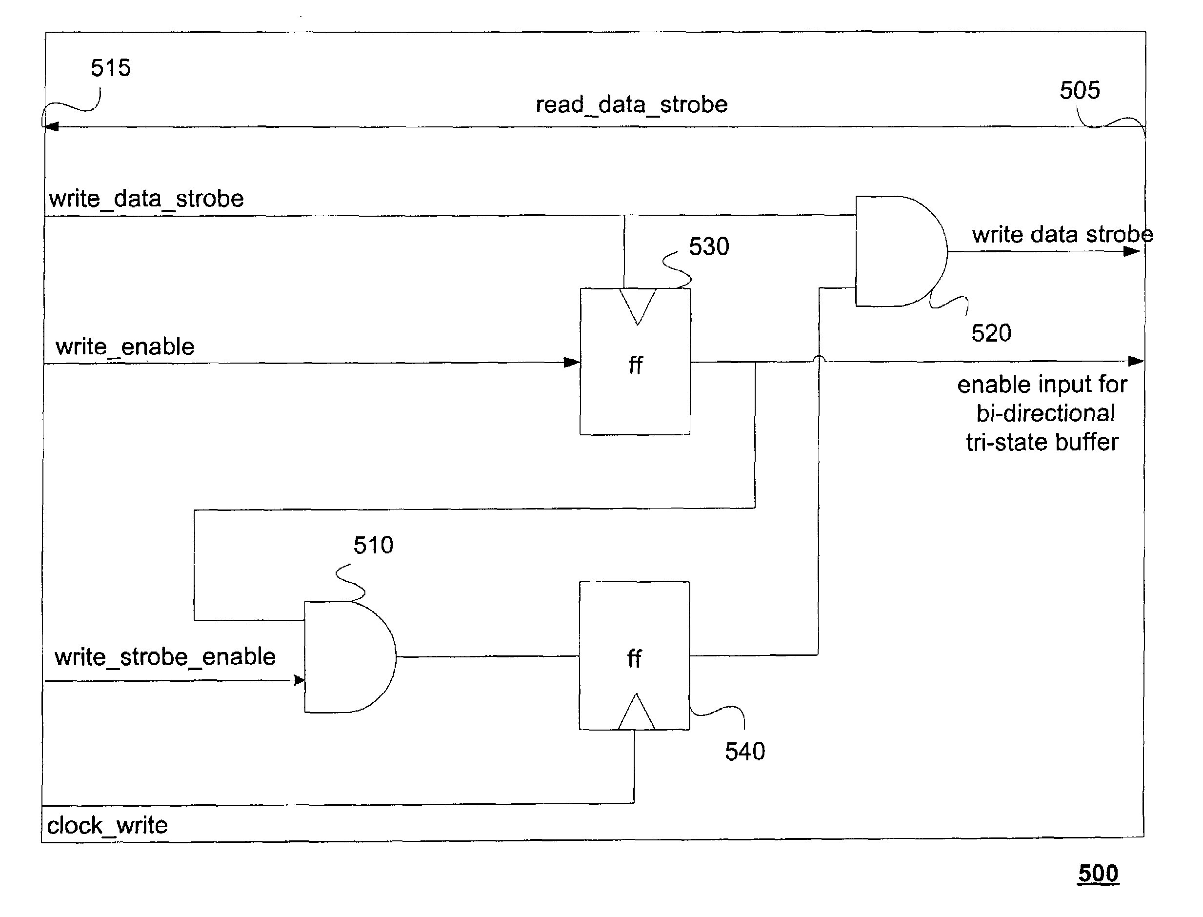
[0032]The present invention provides input / output (I / O) cells that interface between two asynchronous clocking domains. In a preferred embodiment, these I / O cells are used in conjunction with a memory controller that is part of an application specific integrated circuit (ASIC) to interface between the ASIC and a double data rate (DDR) DRAM memory. The memory controller and the I / O cells are used to increase the efficiency of data transfers by outputting the write data, write data strobe and other write commands to the DDR memory with the appropriate timing relationships such that the data can be reliably written to memory.

[0033]FIG. 2A is a block diagram of an application specific integrated circuit (ASIC) 210 coupled to a DDR memory 250. As illustrated, ASIC 210 includes a pad ring 220, a memory controller 230 and the core logic of ASIC 210. Memory controller 230 further comprises delay circuit 240. In one embodiment, delay circuit 240 is a programmable delay compensation circuit (...


PUM


Abstract

An interface for sending write data, write control signals and write data between a memory controller and a double data rate (DDR) memory with the appropriate timing relationships so that the write data can be reliably written in the DDR memory. Also, an interface for reliably capturing read data received from the DDR memory during a read operation.

Description

RELATED APPLICATIONS[0001]This application claims priority under 35 U.S.C. § 119(e) to U.S. Provisional Patent Application Ser. No. 60 / 322,538, “Delay Compensation Circuit for Capturing and Sending DDR Memory Device Data,” by Steven Shrader, Art Gmurowski, Samitinjoy Pal and Michael McKeon, filed Sep. 14, 2001.[0002]This application is related to co-pending U.S. patent application Ser. No. 10 / 211,691, now U.S. Pat. No. 6,665,230, entitled “Programmable Delay Compensation Circuit,” by Steven Shrader, Art Gmurowski, Samitinjoy Pal and Michael McKeon, filed on Jul. 31, 2002, which is herein incorporated by reference.BACKGROUND OF THE INVENTION[0003]1. Field of the Invention[0004]The present invention relates to memory devices and, more particularly, to writing data to and capturing data from Double Data Rate (DDR) memory devices.[0005]2. Description of the Related Art[0006]Double data rate (DDR) memory devices read and write data on both the positive and negative edges (transitions) of...

Claims


Application Information

Patent Timeline
Patent Type & Authority Patents(United States)
IPC IPC(8): G06F12/00
CPCG11C7/1051G11C7/106G11C7/1093G11C7/1078G11C7/1087G11C7/1066
Inventor SHRADER, STEVENGMUROWSKI, ARTPAL, SAMITINJOYMCKEON, MICHAEL
Owner CADENCE DESIGN SYST INC
Why Eureka
Try Eureka