Multi-channel flash memory chip array structure and write-in and read-out methods thereof

A flash memory chip, multi-channel technology, applied in the direction of information storage, static memory, digital memory information, etc., can solve the problem of slow read and write speed of flash memory data, achieve fast read and write speed, high reliability, and ensure the effect of reliability

Active Publication Date: 2014-03-26
雷智数系统技术西安有限公司
View PDF4 Cites 0 Cited by
  • Summary
  • Abstract
  • Description
  • Claims
  • Application Information

AI Technical Summary

Problems solved by technology

[0004] The object of the present invention is to solve the defect of slow reading and writing speed of flash memory data in the prior art, and provide a multi-channel flash memory array structure capable of fast reading and writing flash memory and its writing and reading method

Method used


Image

  • Multi-channel flash memory chip array structure and write-in and read-out methods thereof
  • Multi-channel flash memory chip array structure and write-in and read-out methods thereof
  • Multi-channel flash memory chip array structure and write-in and read-out methods thereof

Examples


Embodiment Construction

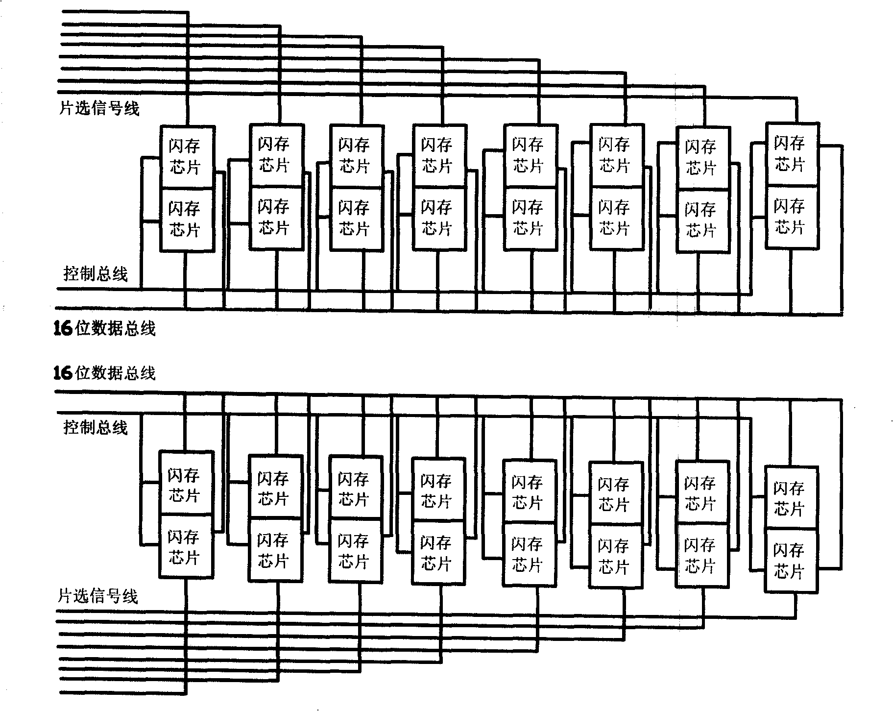
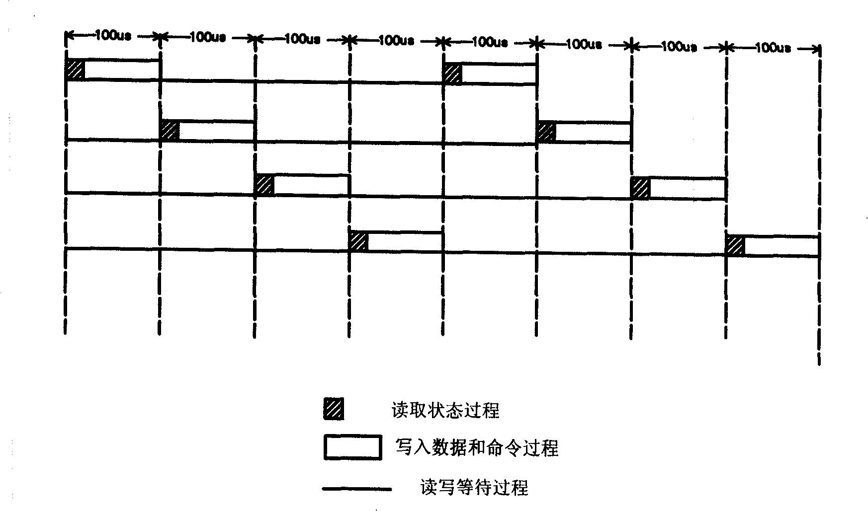
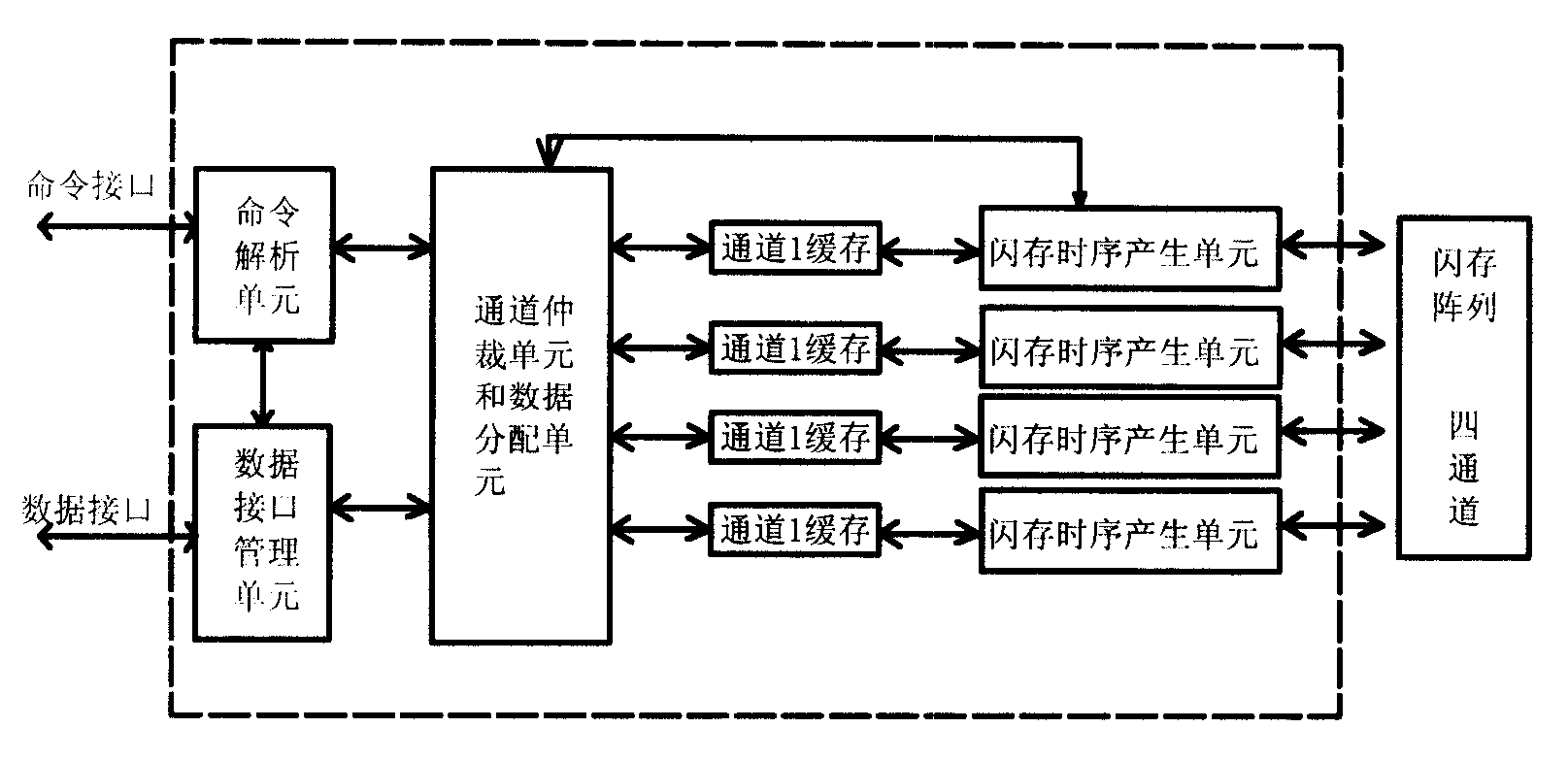
[0037] A multi-channel flash memory chip array structure of the present invention includes a flash memory chip, and multiple channels formed by a data bus, a control bus and a chip selection signal line connected to the flash memory chip, and each flash memory chip corresponds to a chip selection signal line , The chip select signal line of each chip is independent, and all flash memory chips in each channel share a data bus and a control bus independent of other channels. When the flash memory chips in each channel form a flash memory chipset cascade, the chipset is composed of 2 or 4 chips into a 16-bit or 32-bit wide data bus. The purpose of building the chipset is to increase the bit width and increase the unit The writing speed of data within the time, the chips in the chipset share the control bus and the chip select bus, and the data bus is not shared.

[0038] The present invention adopts multi-channel, ie, multi-dimensional array method to manage flash memory chips. For ...


PUM


Abstract

The invention relates to a multi-channel flash memory chip array structure and write-in and read-out methods thereof, which overcome the defect of a slow read-write speed of flash memory data in the prior art. The multi-channel flash memory chip array structure comprises a plurality of channels consisting of flash memory chips, data buses, control buses, and chip selection signal wires, wherein each flash memory chip corresponds to one chip selection signal wire; the chip selection signal wire of each chip is independent; and all the flash memory chips in each channel share one data bus and one control bus which are independent of the other channels. The write-in method comprises the following steps of: transmitting a command and an address message to a command resolving unit through a command interface; starting a data interface management unit and a channel arbitration unit; pre-distributing the channels according to the address message by the channel arbitration unit, and transmitting the data to the channel arbitration unit and a data distribution unit; writing the data in a cache of a corresponding channel, and then starting a corresponding flash memory sequence generation module by the channel arbitration unit; and finally, writing the data into the flash memory chip. The flash memory has a fast write-read speed and high data write-in reliability.

Description

Technical field [0001] The invention relates to a storage device and a writing and reading method thereof, in particular to a multi-channel flash memory array structure and a writing and reading method thereof. Background technique [0002] As a new non-volatile storage medium, flash memory has become very popular in the field of consumer electronics due to its many advantages such as high storage density, easy portability, low power consumption, long data retention time after power failure, and good shock resistance. In the field of industry and military industry, more and more attention and welcome. In some large-capacity data storage applications, multiple flash memories are often cascaded or used as a whole column to expand storage space and improve data throughput. However, the flash memory needs to wait a long time after writing data to ensure that the data is written correctly. Typically, a write needs to wait 200us, and the maximum wait time is 700us. If you follow the...

Claims


Application Information

Patent Timeline
Patent Type & Authority Patents(China)
IPC IPC(8): G11C7/10G06F13/16
Inventor 崔建杰
Owner 雷智数系统技术西安有限公司
Why Eureka
Try Eureka