Semiconductor memory device including write driver and method of controlling the same

a memory device and write driver technology, applied in the direction of information storage, static storage, digital storage, etc., can solve the problem that data to be written may not be properly written, and achieve the effect of improving reliability of write operation, stable write current, and increasing area efficiency

Active Publication Date: 2015-04-28
SK HYNIX INC
View PDF10 Cites 0 Cited by
  • Summary
  • Abstract
  • Description
  • Claims
  • Application Information

AI Technical Summary

Benefits of technology

[0013]In accordance with this technology, a stable write current can be supplied by changing the control scheme of a circuit without a significant change of the circuit. Accordingly, area efficiency can be increased, and the reliability of a write operation can be improved.

Problems solved by technology

In contrast, when a common amount of current is supplied to a memory cell, data to be written may not be properly written.

Method used


Image

  • Semiconductor memory device including write driver and method of controlling the same
  • Semiconductor memory device including write driver and method of controlling the same
  • Semiconductor memory device including write driver and method of controlling the same

Examples


Embodiment Construction

[0018]Hereinafter, a semiconductor memory device and a method of controlling the same according to various embodiments will be described below with reference to the accompanying drawings through the embodiments.

[0019]A phase change memory device from among various semiconductor memory devices is illustrated, but the present invention is not limited thereto. The phase change memory device is described as an example in order to embody an object of the present invention.

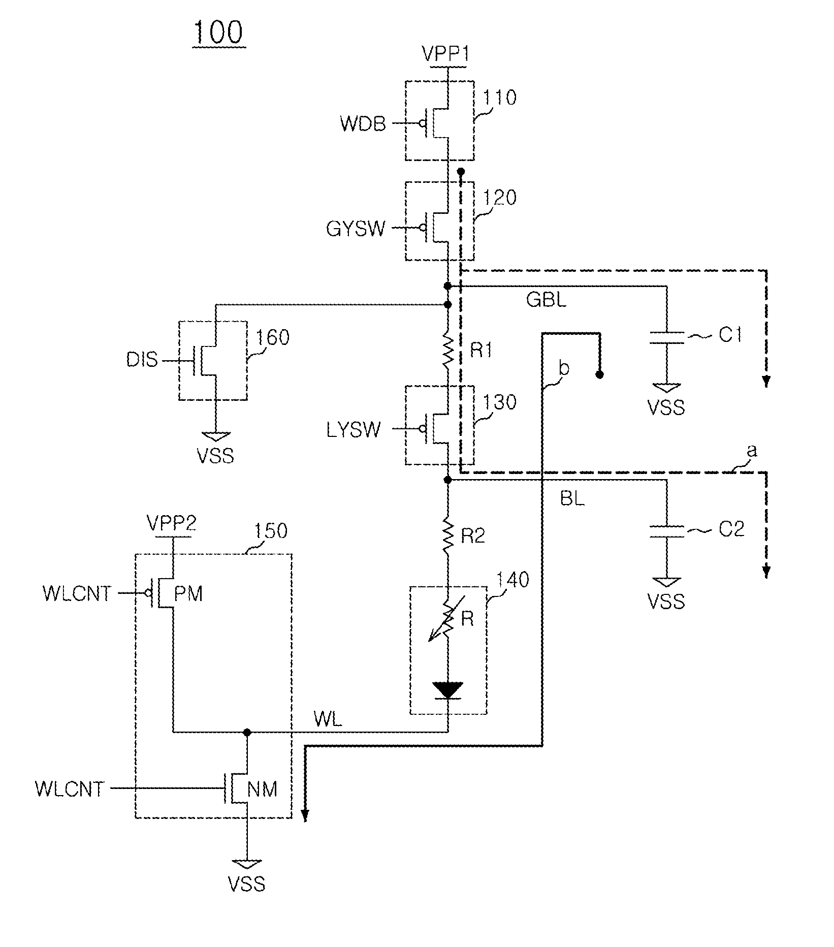
[0020]FIG. 1 shows the construction of a phase change memory device including a write driver in accordance with an embodiment.

[0021]Referring to FIG. 1, the phase change memory device may include a write driver 110, a first switch 120, a second switch 130, a memory cell 140, a word line controller 150, and a discharge unit 160.

[0022]The write driver 110 may be enabled in response to a write driver enable signal WDB (i.e., write command) and configured to include a PMOS. When the write driver 110 is enabled, a first high...


PUM


Abstract

Disclosed is a method of controlling a semiconductor memory device including a write driver. A method of controlling a phase change memory device includes turning on switches connected to a global bit line and a local bit line, respectively, enabling a write driver connected to the switches, enabling a word line, and enabling a memory cell to be accessed by the word line, wherein control is performed so that electric charges supplied from the write driver through the switches are charged when the write driver is enabled.

Description

CROSS-REFERENCES TO RELATED APPLICATION[0001]The present application claims priority under 35 U.S.C. §119(a) to Korean application number 10-2012-0095213, filed on Aug. 29, 2012, in the Korean Intellectual Property Office, which is incorporated herein by reference in its entirety.BACKGROUND[0002]1. Technical Field[0003]The present invention generally relates to a semiconductor memory device and a method of controlling the same, and more particularly, to a semiconductor memory device including a write driver and a method of controlling the same.[0004]2. Related Art[0005]According to a need for an increase in the capacity and speed of semiconductor memory devices and a reduction in the power of semiconductor memory devices, researches are being carried out on the next-generation memory devices which can embody the high degree of integration and low consumption power of DRAM devices, the nonvolatile property of flash memory, and the high-speed operation of SRAM. The next-generation mem...

Claims


Application Information

Patent Timeline
Patent Type & Authority Patents(United States)
IPC IPC(8): G11C7/12G11C7/10
CPCG11C7/12G11C7/1096G11C2207/005G11C13/0004G11C13/0069G11C7/10G11C7/22G11C8/08
Inventor YOON, JUNG HYUKKIM, DONG KEUN
Owner SK HYNIX INC
Why Eureka
Try Eureka