Semiconductor device and power supply using the same

a technology of a power supply and a semiconductor device, which is applied in the direction of dc-dc conversion, power conversion systems, instruments, etc., can solve the problems of insufficient application of a technology to a power supply, insufficient to obtain a high-precision output voltage, and not considered the shift of output voltag

Inactive Publication Date: 2009-10-01
RENESAS ELECTRONICS CORP
View PDF1 Cites 21 Cited by
  • Summary
  • Abstract
  • Description
  • Claims
  • Application Information

AI Technical Summary

Benefits of technology

[0010]More particularly, a semiconductor device for control to be applied to a constant-voltage power supply device supplying a predetermined voltage to a load includes a digital-analog converter circuit outputting a reference voltage corresponding to a value of a first register with taking an output voltage of a reference voltage source as a criterial reference voltage. The digital-analog converter circuit generates a control signal (PWM) for driving a power semiconductor device based on an output voltage of an error amplifier (110) differentially amplifying a feedback voltage (Vfb) and the reference voltage (Vref), which are formed based on the output voltage of the constant voltage power supply device. In this manner, it becomes possible to cancel operation characteristics of the digital-analog converter circuit inside the semiconductor device and an offset of the error amplifier according to the setting value of the first register before embedding the semiconductor device to the constant-voltage power supply device.
[0011]Further, after embedding the semiconductor device in the constant-voltage power supply device, in the case to obtain a feedback voltage by dividing the output voltage of the constant-voltage power supply device by an external voltage dividing resistor circuit (R1, R2), an analog-digital converter circuit (160) which converts the feedback voltage with taking the output voltage of the constant-voltage power supply device as a reference voltage is provided to correct the value of the first register based on an output of the analog-digital converter circuit so as to offset an effect of an error in voltage dividing ratio of the voltage dividing resistor circuit. - The effects obtained by typical aspects of the present invention will be briefly described below.

Problems solved by technology

Meanwhile, although the technique used in the above-mentioned products has setting values of the output voltage in small increments, it has not been considered shifts in the output voltage due to a variation in reference voltage.
In addition, this technique cannot be applied to a power supply including an external voltage dividing resistor and inputting divided voltages to a control IC.
Further, also in the technique disclosed in Patent Documents, there is a variation in resistance values of the adjusting resistors provided in parallel, and it has thus not been sufficient to obtain a high-precision output voltage.

Method used


Image

  • Semiconductor device and power supply using the same
  • Semiconductor device and power supply using the same
  • Semiconductor device and power supply using the same

Examples


first embodiment

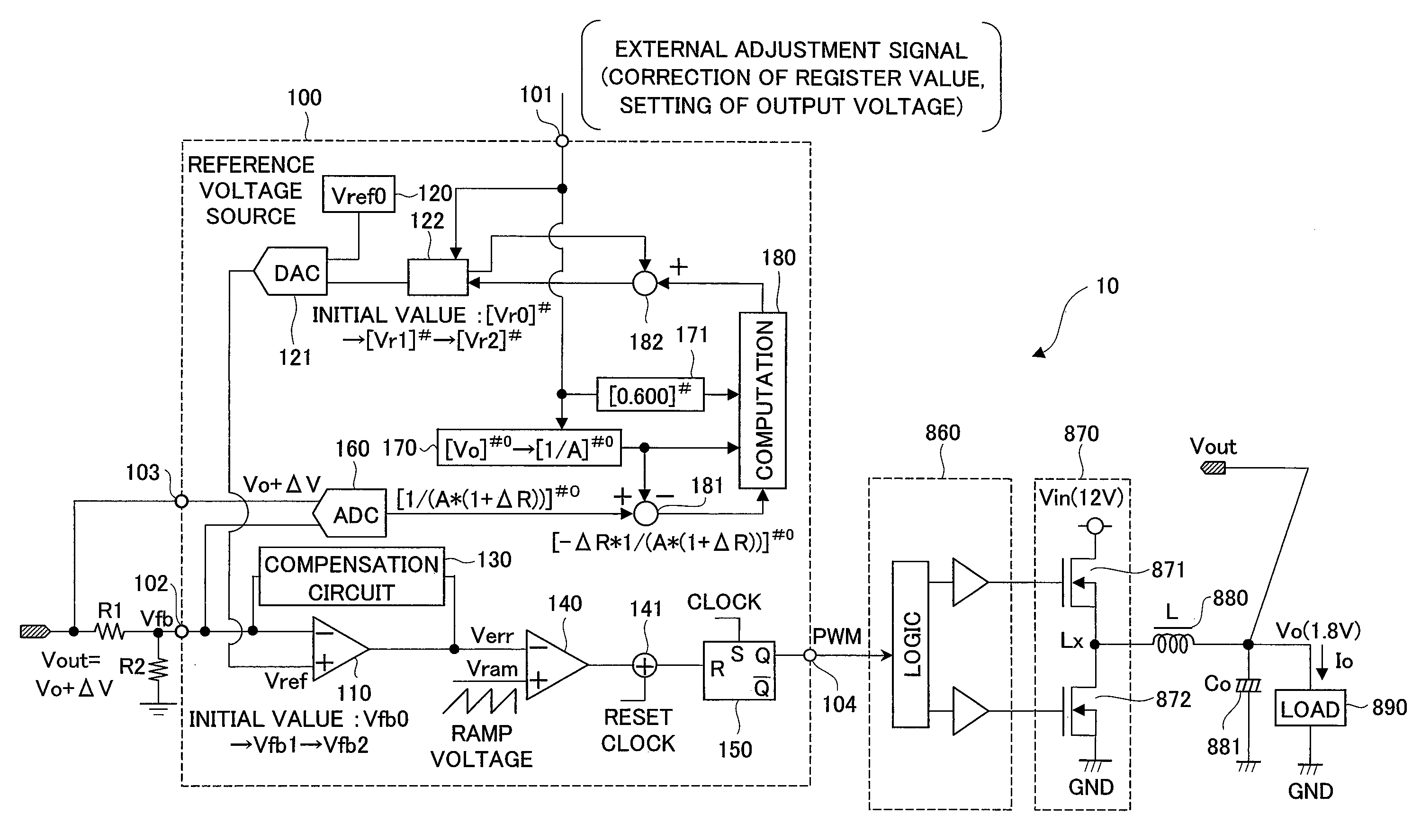
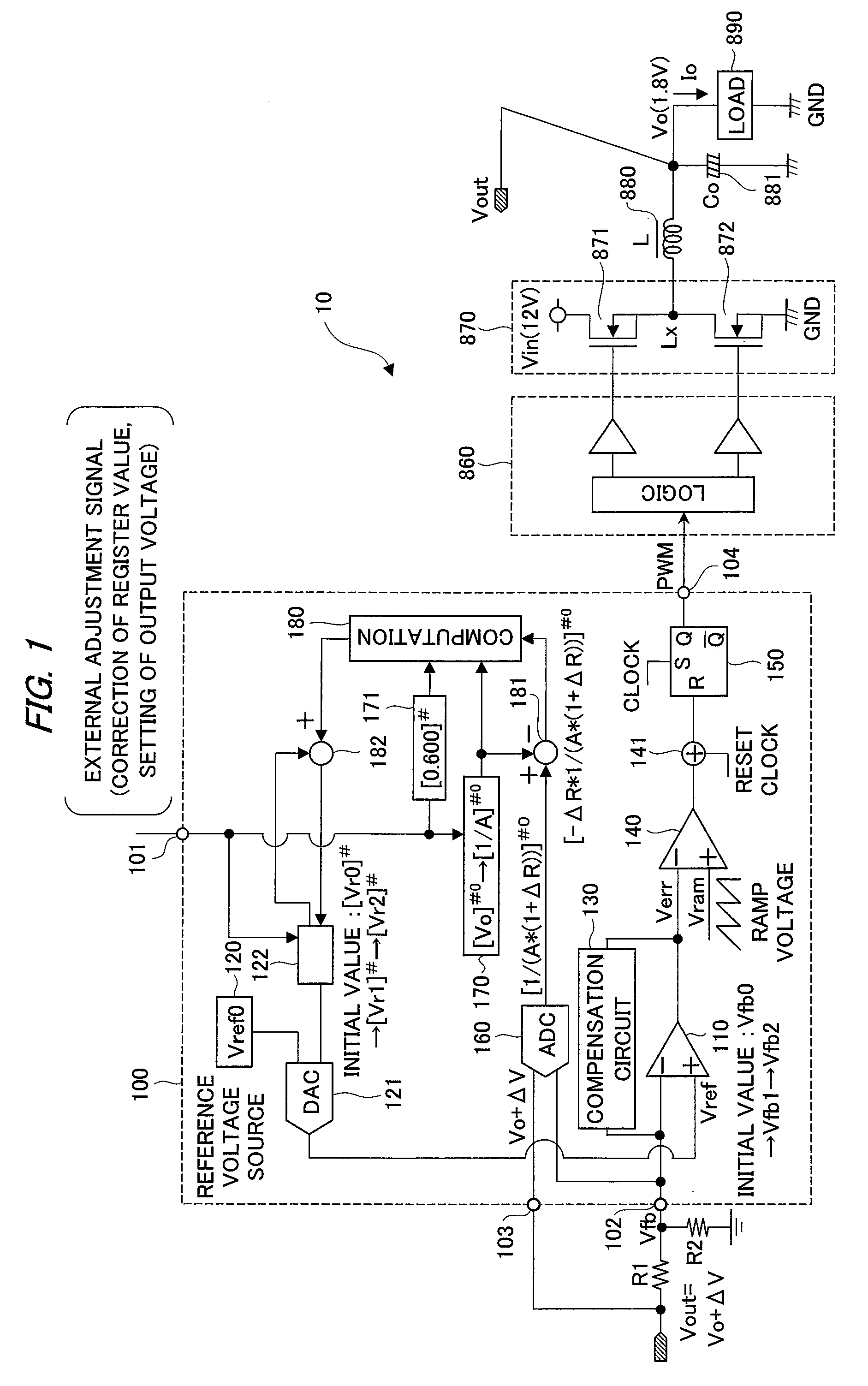
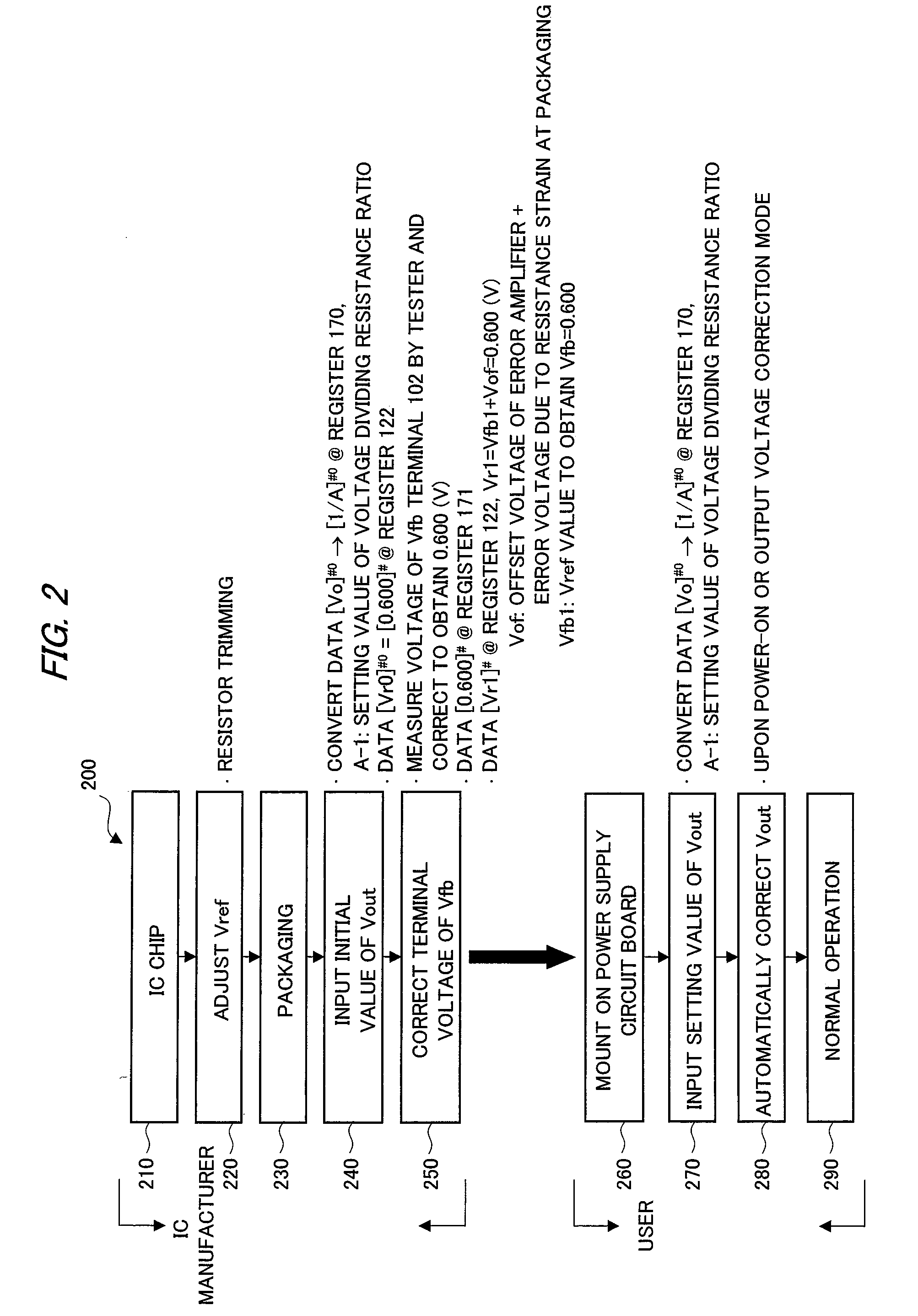
[0043]A first embodiment of the present invention will be described with reference to FIG. 1 to FIG. 4. FIG. 1 is a circuit block diagram of a semiconductor device and a power supply device using the semiconductor device of the first embodiment of the present invention, FIG. 2 is a process chart showing an outline of a process of the semiconductor device of the first embodiment from a chip state to an operation as being embedded on a power supply circuit board, FIG. 3 is an explanatory diagram showing an outline of an automatic Vout correction step, and FIG. 4 is a circuit block diagram showing an example of a digital-analog converter circuit (DAC circuit) used in the semiconductor device of the present invention.

[0044]In FIG. 1, the power supply device (switching power supply device) 10 using the semiconductor device of the first embodiment of the present invention includes: a power supply control IC 100 performing control of pulse width modulation (PWM); a driver circuit 860; a sw...

second embodiment

[0066]A second embodiment of the present invention will be described with reference to FIG. 5. FIG. 5 is a circuit block diagram of a semiconductor device according to the second embodiment of the present invention. A different point from the first embodiment is that the semiconductor device of the second embodiment includes an ADC circuit 410, a register 411, a computing circuit 412, and a switch SW0. These circuits operate to prevent a fluctuation of the output voltage due to a temperature rising in the normal operation mode. The operation will be described hereinafter. At the time point when the correction of the output voltage (step 280 in FIG. 2) is finished, the switch SW0 is turned on to hold the correction value of the register 122 [Vr2]# and the value obtained by converting the output value of the DAC circuit 121 to a digital value [Vfb2]# in the register 411. After holding the values, the switch SW0 is turned off. And, in the normal operation time, a difference between an ...

third embodiment

[0067]A third embodiment of the present invention will be described with reference to FIG. 6 to FIG. 8. FIG. 6 is a circuit block diagram of a semiconductor device according to a third embodiment of the present invention, FIG. 7 is a process chart showing an outline of a process of the semiconductor device of the third embodiment from a chip state through being embedded on a power supply circuit board to an operation, and FIG. 8 is an explanatory diagram showing an outline of an output voltage correction step.

[0068]A different point from the first embodiment is that voltage dividing resistors R3 and R4 are built-in in a power supply control IC 500, and switches SW1 and SW2 used in the output voltage correction are provided. Therefore, a configuration of registers, held data, and a calculation content of a computing circuit 580 are also different from the first embodiment, and the ADC 160 is unnecessary.

[0069]FIG. 7 shows a process chart of an outline of a process of the power supply...


PUM


Abstract

A semiconductor device for control applied to a constant-voltage power supply device includes a digital-analog converter circuit which outputs a reference voltage corresponding to a value of a first register with taking an output voltage of a reference voltage source as a criterial reference voltage, and generates a control signal for driving a power semiconductor device based on an output voltage of an error amplifier which differentially amplifies a feedback voltage obtained by resistive-dividing on an output voltage of the constant-voltage power supply device and the reference voltage. An analog-digital converter circuit which converts the feedback voltage to a digital value with taking the output voltage of the constant-voltage power supply device as a reference voltage is provided, and based on the output, a value of a first register is corrected so as to offset an effect of an error in voltage dividing ratio of a voltage dividing resistor circuit.

Description

CROSS-REFERENCE TO RELATED APPLICATION[0001]The present application claims priority from Japanese Patent Application No. JP 2008-082461 filed on Mar. 27, 2008, the content of which is hereby incorporated by reference into this application.TECHNICAL FIELD OF THE INVENTION[0002]The present invention relates to a semiconductor device technology. More particularly, the present invention relates to a technique effectively applied to a semiconductor device including a power-supply control circuit.BACKGROUND OF THE INVENTION[0003]Regarding a high-precision power supply having a small variation in output voltage, for example, a control IC for high-precision switching power supply has been commercialized, the control IC switching values of a variable resistor embedded in a power-supply control IC chip by using a VID (voltage ID) code of 5-bit or 6-bit, and being capable of setting an output voltage in increments of 25 mV.[0004]In addition, Japanese Patent Application Laid-Open Publication No...

Claims


Application Information

Patent Timeline
Patent Type & Authority Applications(United States)
IPC IPC(8): G05F1/00
CPCH02M2001/0025H02M3/156H02M1/0025
Inventor AKIYAMA, NOBORUHASHIMOTO, TAKAYUKIHIRAO, TAKASHITATENO, KOJIISHIGAKI, TAKUYA
Owner RENESAS ELECTRONICS CORP
Why Eureka
Try Eureka