Apparatus for controlling substrate voltage of semiconductor device

a technology of semiconductor devices and substrate voltage, applied in the direction of individual semiconductor device testing, pulse technique, instruments, etc., can solve the problems of limiting improvement of response, inability to detect change in leakage current, and limitations placed on circuit design, so as to improve the detection sensitivity of leakage current detection circuit, improve response, and improve the effect of controlling substrate voltage precision

Inactive Publication Date: 2010-05-11
PANASONIC SEMICON SOLUTIONS CO LTD
View PDF12 Cites 11 Cited by
  • Summary
  • Abstract
  • Description
  • Claims
  • Application Information

AI Technical Summary

Benefits of technology

[0012]It is therefore an object of the present invention to provide semiconductor integrated circuit apparatus capable of raising detection sensitivity of a leakage current detection circuit and improving response. Further, the present invention provides semiconductor integrated circuit apparatus capable of canceling DC offset error of a comparator and capable of improving precision of controlling substrate voltage.

Problems solved by technology

However, semiconductor integrated circuit apparatus of the related art have the following three problems.
A first problem is that, in the methods of patent document 1 and patent document 2, as these are both methods for detecting fluctuation of drain potential of a leakage current detection NchMOS transistor, if there is no drain potential fluctuation from an initial potential to a potential exceeding a reference potential for detecting fluctuation of drain potential, it is not possible to detect change in leakage current.
This also limits detection sensitivity for leakage current detection and improvement of response.
Further, in a second problem, with the PchMOS transistor substrate voltage control disclosed in patent document 2, restrictions exist in connecting a drain of a PchMOSFET for monitor use and drains of a plurality of PchMOSFETs or NchMOSFETs of an integrated circuit body to an earth potential VSS terminal.
This results in the drawback of limitations such as circuit connection limitations being placed on the circuit design.
Further, in a third problem with the method of patent document 2 and patent document 3, because a comparator employing a comparator or operation amplifier is used, a DC offset error of the comparator becomes a threshold voltage setting value error.

Method used


Image

  • Apparatus for controlling substrate voltage of semiconductor device
  • Apparatus for controlling substrate voltage of semiconductor device
  • Apparatus for controlling substrate voltage of semiconductor device

Examples


first embodiment

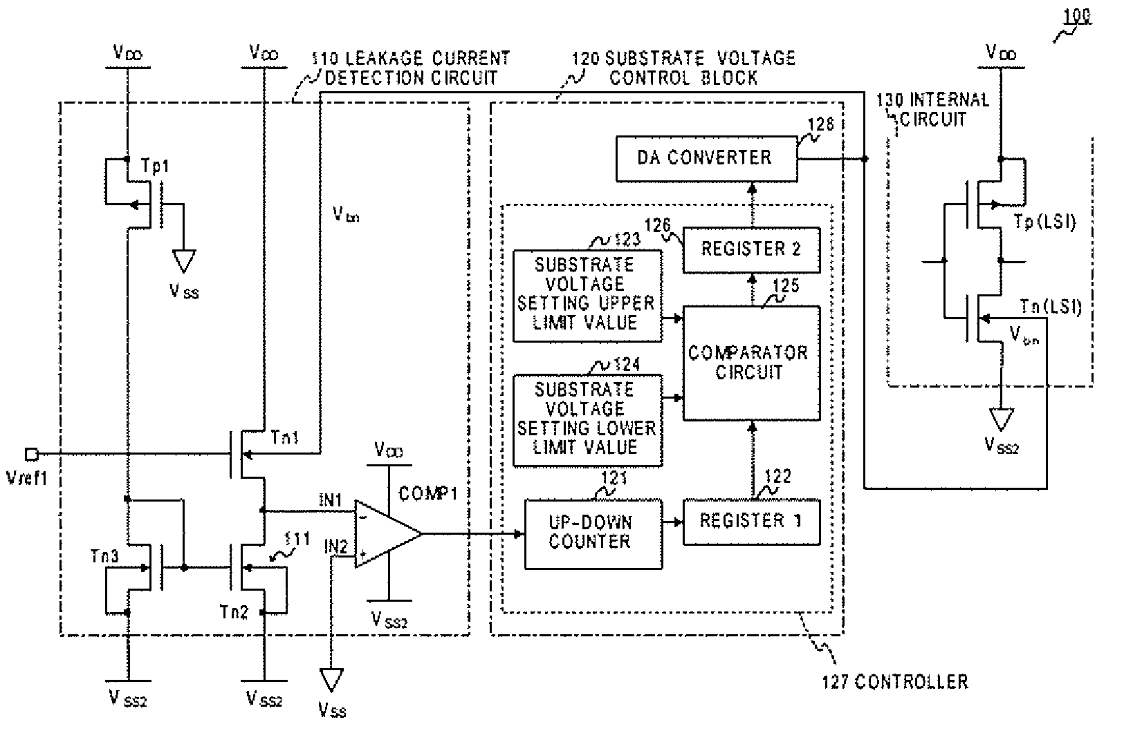
[0042]FIG. 1 is a view showing a configuration of a semiconductor integrated circuit apparatus of a first embodiment of the present invention based on the aforementioned basic concepts. In this embodiment, an example is given of application to semiconductor integrated circuit apparatus equipped with an NchMOS transistor leakage current detection circuit, substrate voltage control block, and internal circuit.

[0043]In FIG. 1, semiconductor integrated circuit apparatus 100 is comprised of NchMOS transistor leakage current detection circuit 110, substrate voltage control block 120 carrying out substrate voltage control, and internal circuit 130 having a plurality of MOS transistors on the semiconductor substrate. Semiconductor integrated circuit apparatus 100 controls the threshold voltage of NchMOS transistors constituting internal circuit 130.

[0044]Leakage current detection circuit 110 is comprised of leakage current detection NchMOS transistor Tn1 with a drain connected to the VDD te...

second embodiment

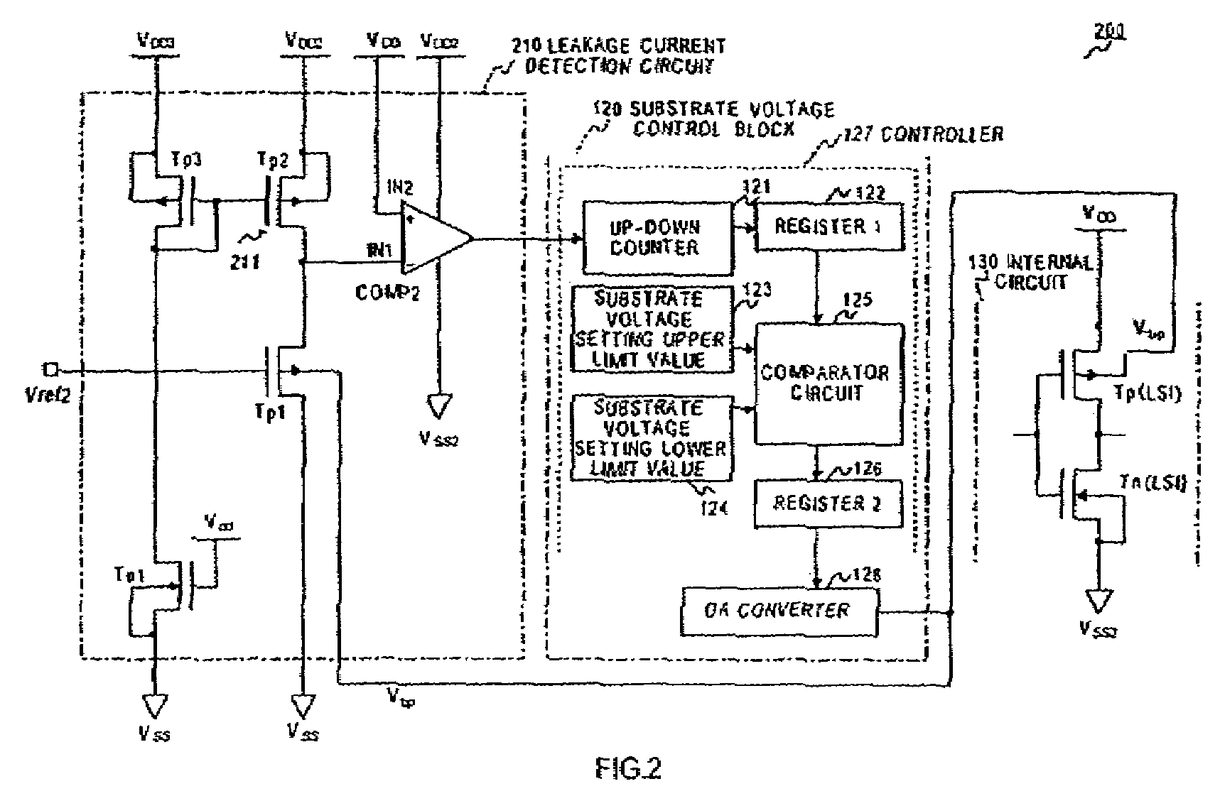
[0061]A second embodiment is an example applied to a leakage current detection circuit employing a leakage current detection PchMOS transistor.

[0062]FIG. 2 is a view showing a configuration for a semiconductor integrated circuit apparatus of a second embodiment of the present invention. In this embodiment, an example is given of application to semiconductor integrated circuit apparatus equipped with a PchMOS transistor leakage current detection circuit, substrate voltage control block, and internal circuit. Portions with the same configuration as for FIG. 1 are given the same numerals and are not described.

[0063]In FIG. 2, semiconductor integrated circuit apparatus 200 is comprised of PchMOS transistor leakage current detection circuit 210, substrate voltage control block 120, and internal circuit 130, and semiconductor integrated circuit apparatus 200 controls the threshold voltages of PchMOS transistors constituting internal circuit 130.

[0064]Leakage current detection circuit 210 ...

third embodiment

[0080]In a third embodiment, an example is given of respectively controlling substrate voltage of a PchMOS transistor and an NchMOS transistor constituting a CMOS circuit at the internal circuit using the semiconductor integrated circuit apparatus of both the first and second embodiments.

[0081]FIG. 3 is a view showing a configuration for a semiconductor integrated circuit apparatus of a third embodiment of the present invention. Portions with the same configuration as for FIG. 1 and FIG. 2 are given the same numerals and are not described.

[0082]In FIG. 3, semiconductor integrated circuit apparatus 300 is comprised of NchMOS transistor leakage current detection circuit 110, PchMOS transistor leakage current detection circuit 210, two substrate voltage control blocks 120, and internal circuit 130, and semiconductor integrated circuit apparatus 300 controls the threshold voltage of an NchMOS transistor and PchMOS transistor constituting internal circuit 130.

[0083]In this way, according...


PUM


Abstract

Semiconductor integrated circuit apparatus capable of raising detection sensitivity of a leakage current detection circuit and improving response. A semiconductor integrated circuit apparatus has a substrate voltage control block that supplies a substrate voltage to an internal circuit and controls NchMOS transistor threshold voltage of the internal circuit, and a leakage current detection circuit constituted by a leakage current detection NchMOS transistor supplied with a high potential side supply voltage to a drain, that has a source connected to a constant current source, and that is applied with an arbitrary stabilizing potential to a gate in such a manner that the substrate voltage is controlled by the substrate voltage control block, and a comparator comparing the source potential of the leakage current detection NchMOS transistor and a predetermined reference potential.

Description

BACKGROUND OF THE INVENTION[0001]1. Field of the Invention[0002]The present invention relates to a semiconductor integrated circuit apparatus that controls MIS (Metal Insulated Semiconductor) transistor threshold voltage, and particularly relates to a semiconductor integrated circuit apparatus capable of controlling substrate voltage of fine-detailed MIS transistors operating at low power supply voltages.[0003]2. Description of the Related Art[0004]In recent years, methods of lowering power supply voltage are well-known as important methods for making semiconductor integrated circuits low in power consumption. However, by lowering the power supply voltage, fluctuations in threshold voltages of MIS transistors or MOS (Metal Oxide Semiconductor) transistors have a substantial influence on operating speed of semiconductor integrated circuits.[0005]With regards to this problem, in the related art, circuit technology for making variations in threshold voltage small has been developed. Fo...

Claims


Application Information

Patent Timeline
Patent Type & Authority Patents(United States)
IPC IPC(8): G01R31/26
CPCG01R31/2621H03K17/6872H03K17/302H03K2217/0018
Inventor ITO, MINORU
Owner PANASONIC SEMICON SOLUTIONS CO LTD
Why Eureka
Try Eureka