Organic light emitting display panel and fabrication method therefor

一种发光显示、制作方法的技术,应用在半导体/固态器件制造、电气元件、电固体器件等方向,能够解决低温多晶硅薄膜晶体管漏电高、无法实现电路关闭效果、OLED发光不稳定等问题,达到优电路关闭效果、发光稳定、光照可靠性好的效果

Inactive Publication Date: 2017-05-31
TCL CHINA STAR OPTOELECTRONICS TECH CO LTD
View PDF3 Cites 21 Cited by
  • Summary
  • Abstract
  • Description
  • Claims
  • Application Information

AI Technical Summary

Problems solved by technology

However, when the metal oxide semiconductor thin film transistor is used as the driving thin film transistor, the current provided by the metal oxide semiconductor thin film transistor to the OLED will be unstable, resulting in unstable light emission of the OLED; and when the low temperature polysilicon thin film transistor is used as the introduction When switching the thin film transistor with the voltage signal sent from the outside, the leakage current of the low temperature polysilicon thin film transistor is high, so that a better circuit closing effect cannot be achieved

Method used


Image

  • Organic light emitting display panel and fabrication method therefor
  • Organic light emitting display panel and fabrication method therefor
  • Organic light emitting display panel and fabrication method therefor

Examples


Embodiment Construction

[0022] Hereinafter, embodiments of the present invention will be described in detail with reference to the accompanying drawings. This invention may, however, be embodied in many different forms and should not be construed as limited to the specific embodiments set forth herein. Rather, the embodiments are provided to explain the principles of the invention and its practical application, thereby enabling others skilled in the art to understand the invention for various embodiments and with various modifications as are suited to particular intended uses.

[0023] In the drawings, the thicknesses of layers and regions are exaggerated for device clarity. Like reference numerals refer to like components throughout the specification and drawings.

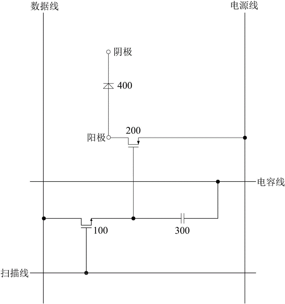
[0024] figure 1 is a pixel circuit diagram of an OLED display panel according to an embodiment of the present invention.

[0025] refer to figure 1 , in the active OLED display panel, the active driving method is to have TFT and stor...


PUM


Abstract

The invention discloses an organic light emitting display panel. The organic light emitting display panel comprises a substrate and a driving thin film transistor, a switching thin film transistor, a storage capacitor and an organic light emitting device which are formed on the substrate; an external voltage signal passes through the switching thin film transistor to be stored in the storage capacitor; the external voltage signal controls the size of the conduction current of the driving thin film transistor so as to control the gray scale of the organic light emitting device; the driving thin film transistor is a low-temperature polysilicon thin film transistor; and the switching thin film transistor is a metal oxide semiconductor thin film transistor. The invention also discloses a fabrication method for the organic light emitting display panel. According to the organic light emitting display panel and the fabrication method therefor, the drain of the low-temperature polysilicon thin film transistor is in contact with the bottom electrode of the organic light emitting device, so that the current supplied for the organic light emitting device is stable, and the organic light emitting device can realize stable light emitting; and meanwhile, the electrical leakage of the metal oxide semiconductor thin film transistor is relatively low, so that a better circuit closing effect can be realized.

Description

technical field [0001] The invention belongs to the technical field of organic light-emitting display, and in particular relates to an organic light-emitting display panel and a manufacturing method thereof. Background technique [0002] In recent years, organic light-emitting diode (Organic Light-Emitting Diode, OLED) display panel has become a very popular emerging flat display panel product at home and abroad. Time (1μs), high luminous efficiency, wide color gamut, low operating voltage (3 ~ 10V), thin thickness (less than 1mm), can make large-sized and flexible panels and simple manufacturing process, and it also has Low cost potential. [0003] Existing OLED display panels can be classified into passive OLED display panels (PM-OLED) and active OLED display panels (AM-OLED) according to their driving methods. In an active OLED display panel, a thin film transistor (TFT) is usually used together with a capacitor to store signals to control the brightness grayscale perfo...

Claims


Application Information

Patent Timeline
Patent Type & Authority Applications(China)
IPC IPC(8): H01L27/32H01L21/82
CPCH01L21/82H10K59/124H01L27/1251H01L27/1255H01L27/1259H01L29/7869H01L29/78675H01L27/1225H10K59/1213H10K59/1201
Inventor 周星宇迟世鹏
Owner TCL CHINA STAR OPTOELECTRONICS TECH CO LTD
Why Eureka
Try Eureka