Reduced size semiconductor package with stacked dies

a technology of stacked dies and semiconductors, applied in the field of semiconductor packages, can solve the problems of reducing or diminishing the utility of certain applications, structural limits, and limited ability of current known semiconductor packages including only a single semiconductor die to perform multi-functions, etc., and achieve the effect of facilitating a reduction in the size of the semiconductor packag

Inactive Publication Date: 2005-08-09
AMKOR TECH SINGAPORE HLDG PTE LTD
View PDF117 Cites 188 Cited by
  • Summary
  • Abstract
  • Description
  • Claims
  • Application Information

AI Technical Summary

Benefits of technology

[0009]In the semiconductor package of the present invention, the first semiconductor die and the leads are oriented relative to each other such that each of the bond pads of the first semiconductor die is located between a respective pair of the leads. As such, the bond pads of the first semiconductor die do not contact the second surface of any one of the leads. The conductive wires electrically connecting the bond pads of the first semiconductor die to the leads are thus oriented inwardly relative to the peripheral edge of the first semiconductor die. This relative orientation facilitates a reduction in the size of the semiconductor package.

Problems solved by technology

However, those currently known semiconductor packages including only a single semiconductor die are limited in their ability to perform multi-functions.
However, these semiconductor packages have structural limits attributable to the stacking of the dies or packages therein, and are often of a size which decreases or diminishes their utility in certain applications.

Method used


Image

  • Reduced size semiconductor package with stacked dies
  • Reduced size semiconductor package with stacked dies
  • Reduced size semiconductor package with stacked dies

Examples


Embodiment Construction

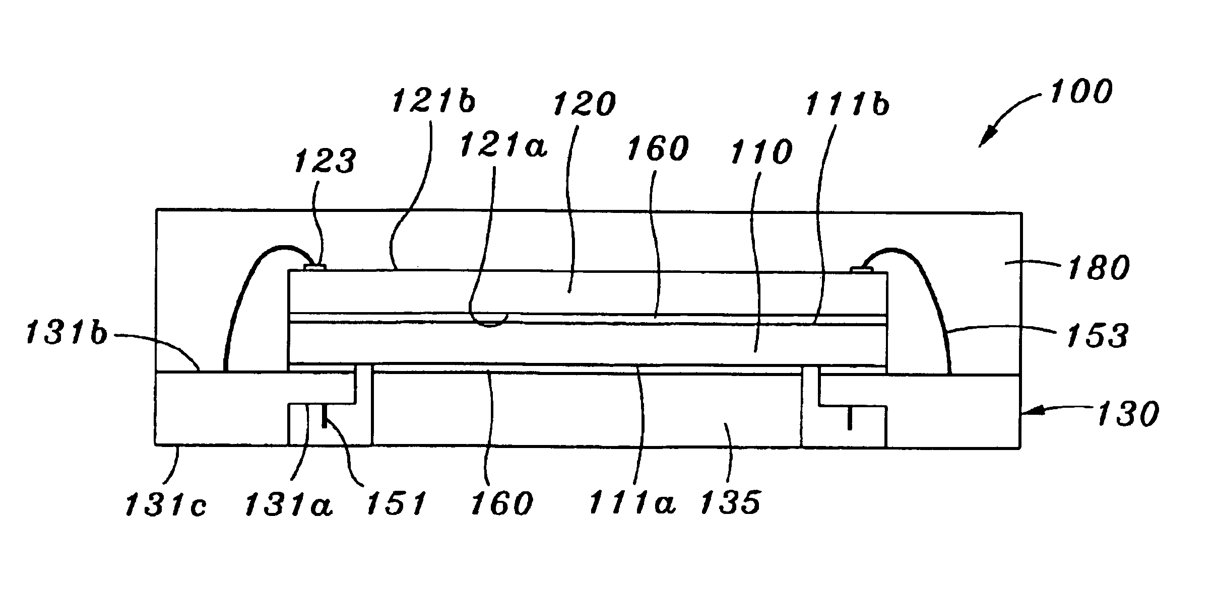
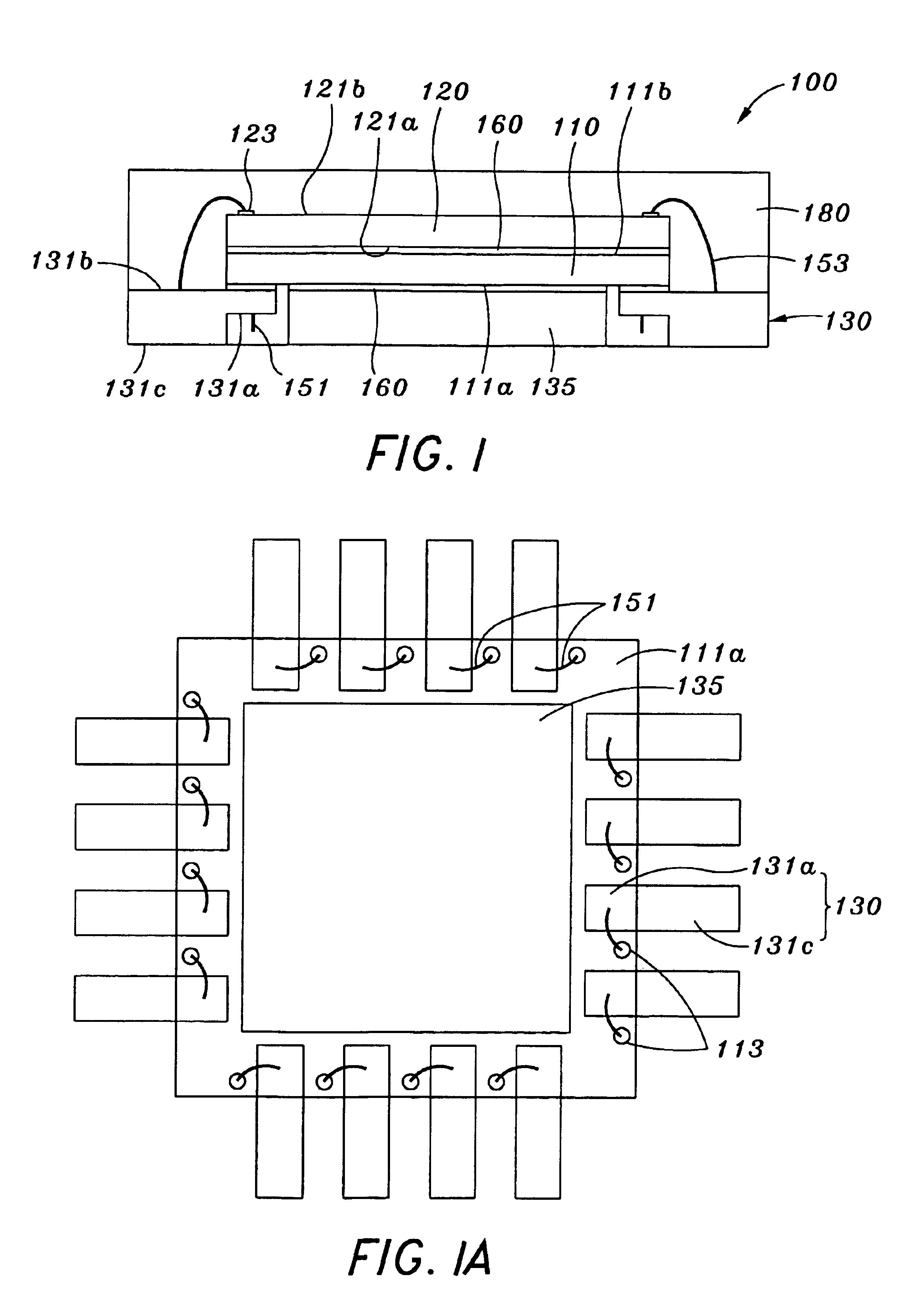
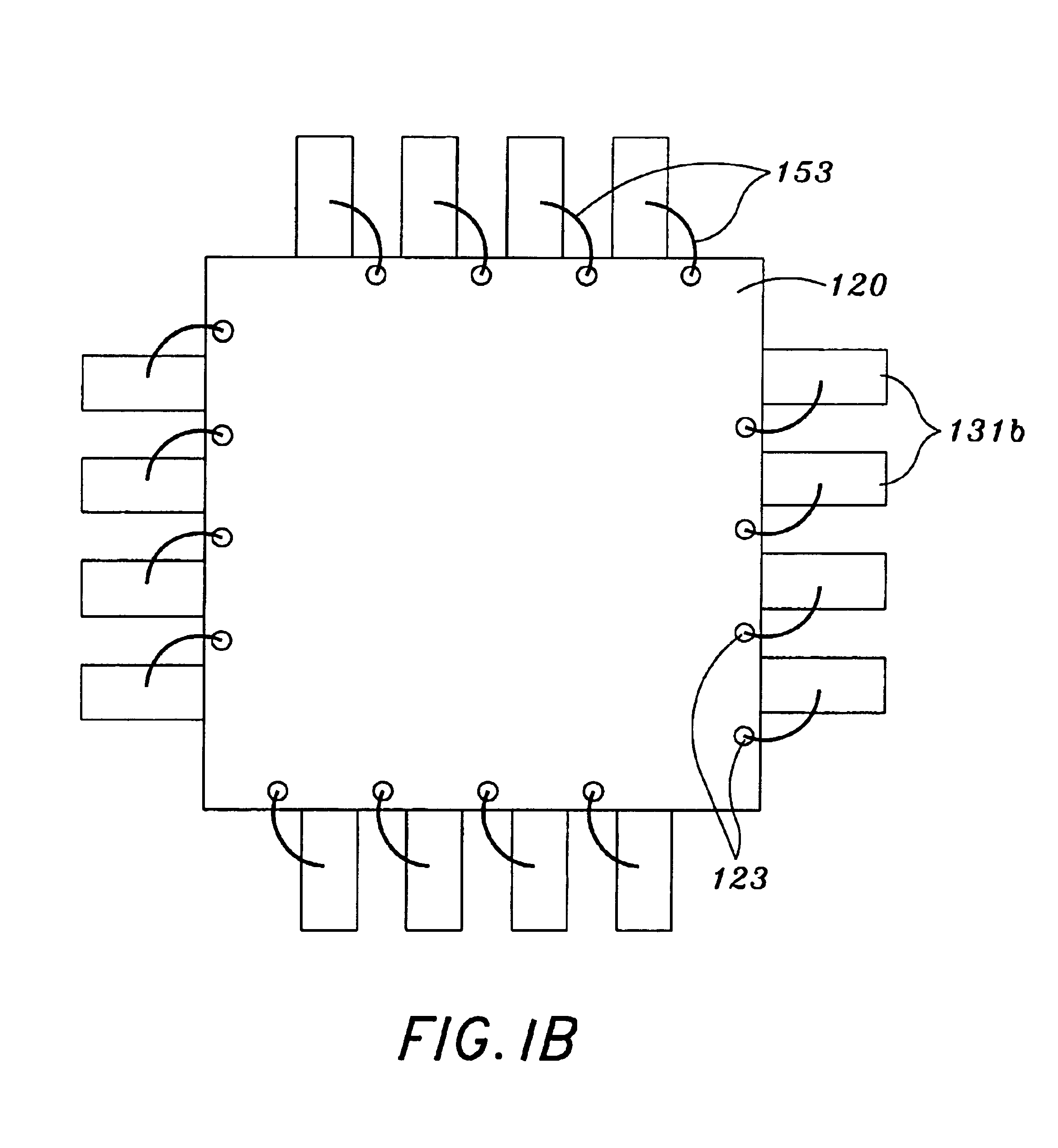
[0017]Referring now to the drawings wherein the showings are for purposes of illustrating a preferred embodiment of the present invention only, and not for purposes of limiting the same, FIG. 1 provides a cross-sectional view of a semiconductor package 100 constructed in accordance with the present invention. The semiconductor package 100 comprises a plurality of identically configured leads 130. Each of the leads 130 defines a generally planar first (lower) surface 131a and a generally planar second (upper) surface 131b which is disposed in opposed relation to the first surface 131a. Each lead 130 further defines a generally planar third (lower) surface 131c which is also disposed in opposed relation to the second surface 131b and is laterally offset outwardly relative to the first surface 131a. More particularly, the thickness between the second and third surfaces 131b, 131c exceeds the thickness between the first and second surfaces 131a, 131b. The first surfaces 131a of the lead...


PUM


Abstract

A semiconductor package comprising a plurality of leads. Each of the leads defines opposed first and second surfaces, and a third surface which is also disposed in opposed relation to the second surface. The first surface is oriented between the second and third surfaces. The semiconductor package further comprises first and second semiconductor dies which each define opposed first and second surfaces. Disposed on the first surface of the first semiconductor die are a plurality of bond pads, with bond pads also being disposed on the second surface of the semiconductor die. The first surface of the first semiconductor die is attached to the second surface of each of the leads, with the first surface of the second semiconductor die being attached to the second surface of the first semiconductor die. A plurality of conductive connectors or wires electrically connect the bond pads of the first and second semiconductor dies to respective ones of the leads. An encapsulating portion is applied to and at least partially encapsulates the leads, the first and second semiconductor dies, and the conductive connectors.

Description

CROSS-REFERENCE TO RELATED APPLICATIONS[0001]The present application claims priority to Korean Patent Application No. 2001-02163 entitled SEMICONDUCTOR PACKAGE filed Jan. 15, 2001.STATEMENT RE: FEDERALLY SPONSORED RESEARCH / DEVELOPMENT[0002](Not Applicable)BACKGROUND OF THE INVENTION[0003]1. Field of the Invention[0004]The present invention relates generally to semiconductor packages, and more particularly to a semiconductor package which includes a stacked pair of semiconductor dies, one of which is electrically connected to the leads of the semiconductor package in a manner facilitating a reduction in the size of the semiconductor package.[0005]2. Description of the Related Art[0006]As is well known in the electrical arts, recent advances in semiconductor package technology have led to the development of packaging techniques which provide for the continuing miniaturization of the semiconductor package. These advancements have also led to the development of a wide variety of new and...

Claims


Application Information

Patent Timeline
Patent Type & Authority Patents(United States)
IPC IPC(8): H01L23/28H01L23/31H01L23/495H01L23/48H01L23/12
CPCH01L23/3107H01L23/49548H01L23/49575H01L24/32H01L24/83H01L2224/45124H01L2924/00014H01L2224/45144H01L2224/48091H01L2224/73265H01L2224/32245H01L2224/48247H01L24/45H01L24/85H01L2224/48227H01L2224/48465H01L2224/49171H01L2224/8319H01L2224/8385H01L2224/92247H01L2924/01005H01L2924/01013H01L2924/01075H01L2924/01079H01L2924/01082H01L2924/07802H01L24/48H01L24/49H01L2224/2919H01L2924/01006H01L2924/01033H01L2924/0665H01L2924/00H01L2224/85H01L2924/12041H01L2224/2612H01L2924/181H01L2924/00012H01L23/12
Inventor PAEK, JONG SIK
Owner AMKOR TECH SINGAPORE HLDG PTE LTD
Why Eureka
Try Eureka