Flat-panel display and flat panel display cathode manufacturing method

a manufacturing method and flat panel technology, applied in the manufacture of discharge tubes/lamps, tubes with screens, discharge tubes luminescent screens, etc., can solve the problems of non-uniform amount of electrons emitted, failure to form flat cathodes, irregular luminance, etc., and achieve the effect of free from luminance irregularities

Inactive Publication Date: 2005-09-13
NORITAKE CO LTD
View PDF13 Cites 33 Cited by
  • Summary
  • Abstract
  • Description
  • Claims
  • Application Information

AI Technical Summary

Benefits of technology

[0004]It is an object of the present invention to provide a flat-panel display which is free from luminance irregularity e...

Problems solved by technology

In the above conventional flat-panel display, however, cathodes formed by printing vary in thickness or a surface undulation occurs, resulting in failure to form flat cathodes.
In such a case, when field electron emission is caused by using parallel electric fields, the electric fields...

Method used


Image

  • Flat-panel display and flat panel display cathode manufacturing method
  • Flat-panel display and flat panel display cathode manufacturing method
  • Flat-panel display and flat panel display cathode manufacturing method

Examples


first embodiment

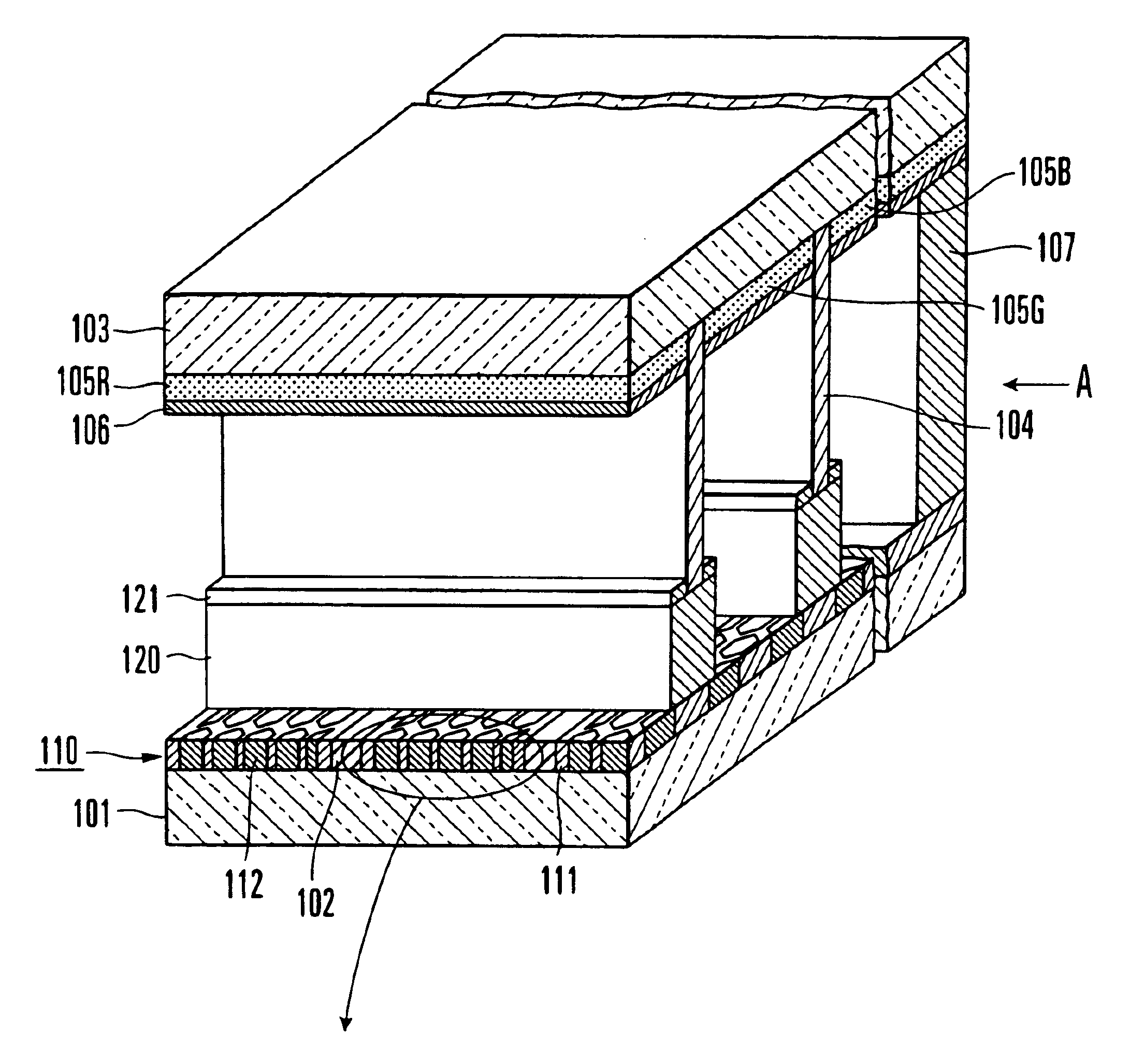
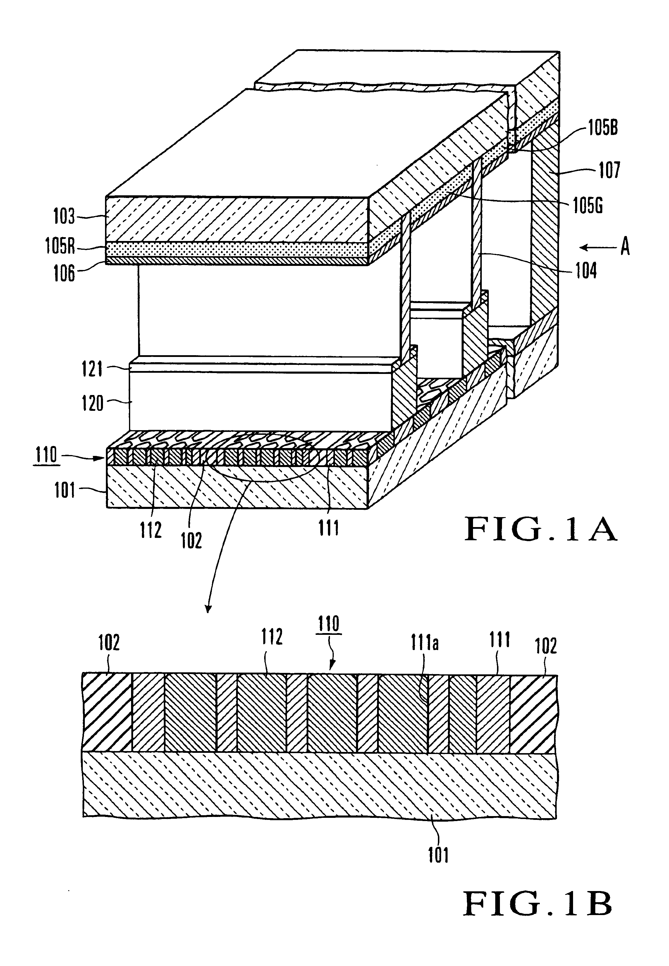
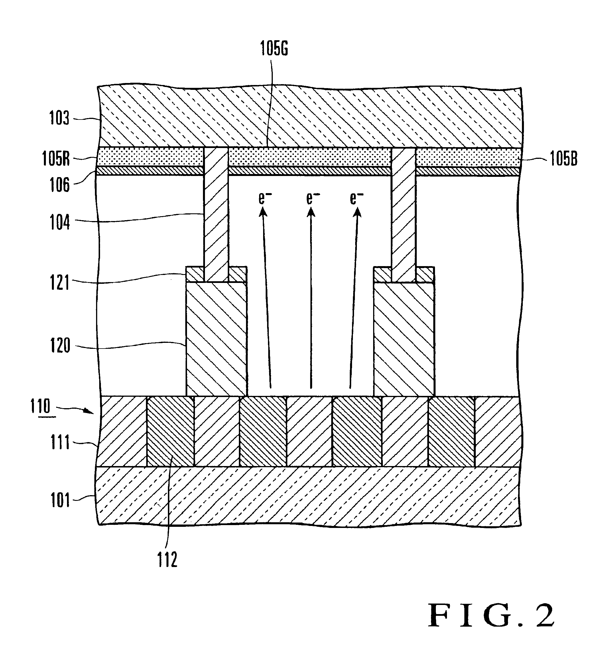
[0013]FIGS. 1A and 1B show the arrangement of a flat-panel display according to the present invention. As shown in FIG. 1A, the flat-panel display according to this embodiment includes a glass substrate 101 having a substantially rectangular shape when viewed from the top, a transparent front glass 103 which is placed to oppose the glass substrate 101 at a predetermined distance and has a substantially rectangular shape when viewed from the top, and a frame-like spacer glass 107 placed on the peripheral portions of these components. The spacer glass 107 is bonded to the peripheral portions of the glass substrate 101 and front glass 103, which are placed to oppose each other, with low-melting frit glass to form an envelope. The envelope is held at a vacuum degree of 10−5 Pa. Low alkaline soda glass is used for the glass substrate 101, front glass 103, and spacer glass 107 which constitute the envelope. Plate glass members each having a thickness of 1 to 2 mm are used as the glass sub...

second embodiment

[0040]FIG. 5 shows the structure of a flat-panel display according to the present invention. As in this embodiment, front-surface ribs 104 may be formed in a direction perpendicular to insulating spacers 120. In this case, gate electrodes 122 formed on the insulating spacers 120 are formed from split electrodes which are split by the front-surface ribs 104 in the longitudinal direction of the insulating spacers 120 and electrically connected to each other.

[0041]In the above embodiment, the surface of the conductive film in each mesh-like opening portion 111a is irradiated with a laser beam to expose carbon nanotubes. However, a method of exposing carbon nanotubes is not limited to the laser beam irradiation method. For example, carbon nanotubes may be exposed by selective dry etching using a plasma. In addition, the glass substrate is used as a component of the envelope. However, a ceramic substrate or the like may be used.

[0042]Furthermore, the conductive paste 116 is obtained by k...


PUM


Abstract

A flat-panel display includes a front glass, glass substrate, cathodes, gate electrodes, phosphor films, and anodes. The front glass has translucency at least partly. The substrate is placed to oppose the front glass through a vacuum space. The cathodes are formed on the substrate. The gate electrodes are placed in the vacuum space and spaced apart from the cathodes. The phosphor layers and anodes are formed on a surface of the front glass which opposes the substrate. Each cathode includes a metal member having many opening portions which is mounted on the substrate, and a conductive material containing carbon nanotubes filled in the mesh-like opening portions. A method of manufacturing a flat-panel display is also disclosed.

Description

BACKGROUND OF THE INVENTION[0001]The present invention relates to a flat-panel display which emits light by bombarding electrons emitted from a field emission electron source against a phosphor and a method of manufacturing a flat-panel display cathode.[0002]As one of the electron display devices, a flat-panel display such as an FED (Field Emission Display) or flat fluorescent display tube is available, which emits light by bombarding electrons emitted from an electron-emitting source serving as a cathode against a light-emitting portion formed from a phosphor formed on a counterelectrode. Recently, an electron-emitting source using carbon nanotubes has been proposed as an electron-emitting source for such a flat-panel display. In a conventional flat-panel display using carbon nanotubes as electron-emitting sources, a paste containing carbon nanotubes is printed on a cathode wiring layer formed on a substrate and used as a cathode.[0003]In the above conventional flat-panel display, ...

Claims


Application Information

Patent Timeline
IPC IPC(8): H01J63/00H01J31/12H01J63/04H01J29/46H01J1/02H01J1/05H01J29/04H01J9/02H01J31/15H01J9/24H01J9/00H01J9/04H01J1/62H01J1/00H01J1/30H01J1/304
CPCB82Y10/00H01J1/304H01J9/025H01J2201/30469H01J2329/00C01B32/05B82Y40/00
Inventor UEMURA, SASHIROYOTANI, JUNKO
Owner NORITAKE CO LTD
Why Eureka
Try Eureka