Semiconductor and device nanotechnology and methods for their manufacture
a technology of semiconductors and devices, applied in the direction of catalyst activation/preparation, metal/metal-oxide/metal-hydroxide catalysts, magnetic materials, etc., can solve the problems of lack of selectivity, lack of real-time monitoring and control, and several inherent limitations of existing sensors, so as to achieve high sensitivity and selectivity for a physical property or analyte
- Summary
- Abstract
- Description
- Claims
- Application Information
AI Technical Summary
Benefits of technology
Problems solved by technology
Method used
Image

Examples
example 1
Growth of Nanoporous Anodic Alumina Substrates
[0072]Pure (99.99% Al) aluminum foil was degreased in spectroscopic grade CC14 in an ultrasonic bath, and then rinsed in deionized water. The foil was immersed into the anodization bath with aluminum counterelectrodes. Anodic voltage was immediately applied to the aluminum substrate. The anodization bath comprised either sulfuric or oxalic acids, depending on the desired pore diameter. Electrolyte compositions, voltages, and temperatures for several specimens are listed in Table 1, as well as the resulting pore sizes.
[0073]
TABLE 1Processing conditions for growth of nanoporous anodic aluminaporeelectrolyteanodizationdiameter,composition,anodizationtemperature,nmM (moles / liter)voltage, V° C.700.25M H2C2O47510500.25M H2C2O45420250.25M H2C2O42720121.2M H2SO4152091.2M H2SO415051.2M H2SO472051.2M H2SO415−20in MeOH
example 2
Fabrication of Three-eElectrode Resistive Sensor Substrates by Anisotropic Etching
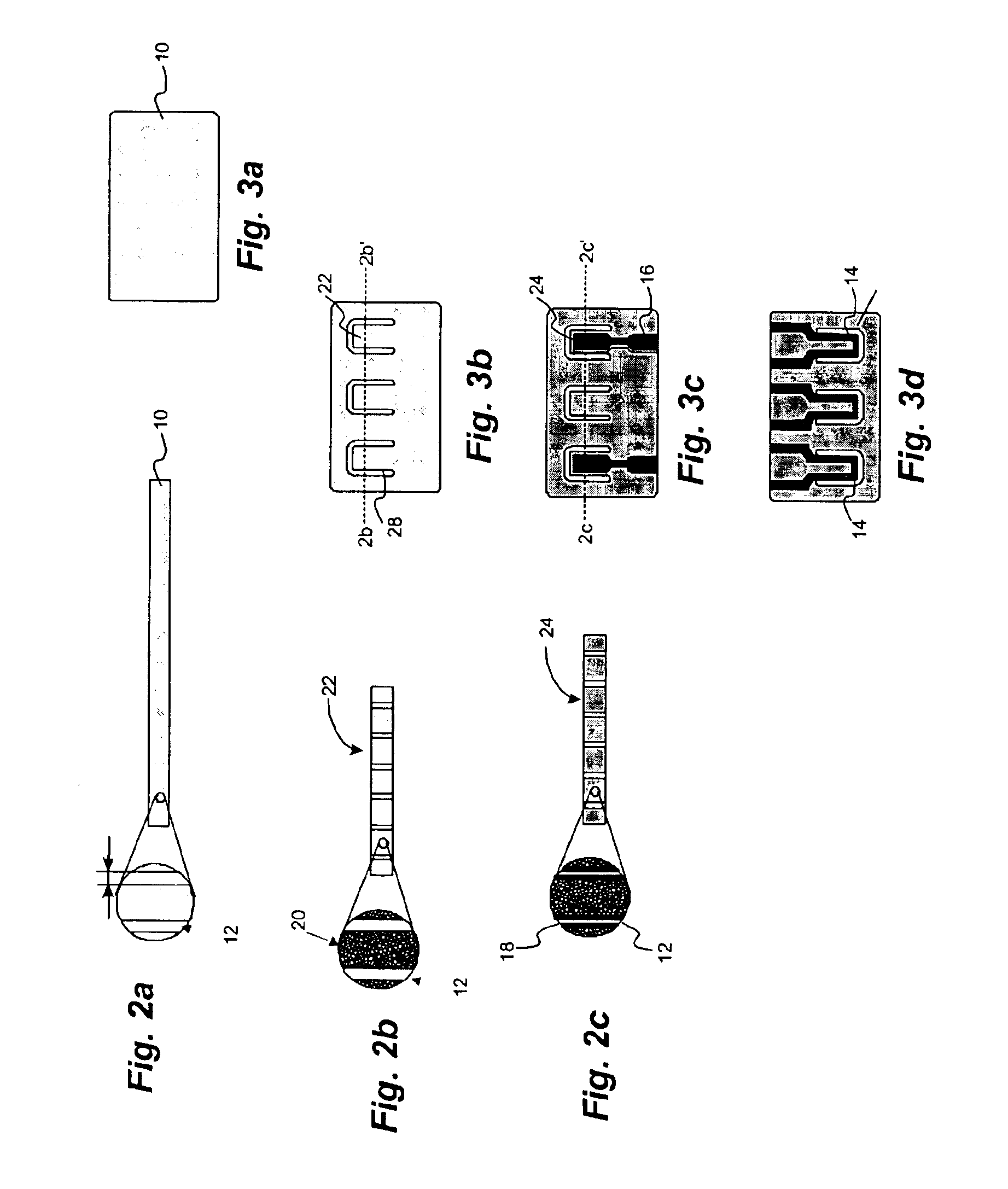
[0074]Nanoporous AAO (Anodized Aluminum Oxide; a.k.a. anodic alumina) films were prepared on both sides of 5 cm×10 cm piece of Al foil as described in the Example 1, resulting in 70 nm pore diameter and 40 micrometer film thickness. A protective layer comprising aluminum and 5% by weight copper, that was 300 nm thick, was plasma sputtered onto both sides of the AAO to close the pores and prevent penetration of the photoresist inside the pores.
[0075]A standard positive photoresist was spin-coated at 4000 rpm and pre-baked at 120° C. for 1 minute. Both sides of the samples were exposed through a contact mask using a mask aligner, and developed in a standard developer solution. Resulting photoresist patterns were hard-baked at 160° for 1 hrs. Exposed areas of the Al / Cu layer were etched in the solution of 5% CuCl2 in 20% HCl to expose anodic alumina surfaces. Exposed AAO was etched in a solution of 200 g / ...
example 3
Fabrication of Three-electrode Sensor Substrates by Localized Anodization
[0077]Nanoporous AAO films were prepared on both sides of 5 cm×10 cm piece of Al foil as described in the Example 1 for 70 nm pore diameter, except the film thickness was limited to 0.25 μm. A standard positive photoresist was spin-coated at 4000 rpm without a protective layer and pre-baked at 120° C. for 1 minute. Both sides of the samples were exposed through a contact mask using a mask aligner, and developed in a standard developer solution. Resulting photoresist pattern was hard-baked at 160° C. for 1 hour. The samples were inserted into a anodization bath, and a second anodization was performed at 75V in exposed areas until additional 40 μm of AAO was grown. At the end of the anodization, the samples were polarized at −100V in the anodization solution until gas evolution was observed in the exposed areas. This procedure opened the barrier layer. The photoresist layers were then stripped in the commercial s...
PUM
| Property | Measurement | Unit |
|---|---|---|
| Composition | aaaaa | aaaaa |
Abstract
Description
Claims
Application Information
 - R&D
- Intellectual Property
- Life Sciences
- Materials
- Tech Scout
- Unparalleled Data Quality
- Higher Quality Content
- 60% Fewer Hallucinations
Browse by: Latest US Patents, China's latest patents, Technical Efficacy Thesaurus, Application Domain, Technology Topic, Popular Technical Reports.
© 2025 PatSnap. All rights reserved.Legal|Privacy policy|Modern Slavery Act Transparency Statement|Sitemap|About US| Contact US: help@patsnap.com